Please find additional clarifications and details in the DP1 FAQ
Update:
A DP1 style guide was distributed in tutorial on March 14. It is available online in pdf or Word doc formats.
6.033 Design Project: NAND Flash Storage Device
There are two deliverables for Design Project 1 (check the course calendar for the due dates):
1. Two copies of a design proposal not exceeding 800 words.
2. Two copies of a design report not exceeding 2,500 words. The design report is due later than the proposal; you will get feedback on the proposal before the due date of the report.
Both deliverables are due at the start of your assigned recitation on the due date.
A design report is a different beast from a quiz: it has no single correct answer. We strongly recommend that you get started early so that you can iterate your design. A good design is likely to take more than just a few days to put together.
The Problem
In this project you will design a flash storage system. The system that you design will serve as the core of flash-based storage devices like USB memory sticks and flash memory cards. The following diagram shows the overall structure of a computer connected to a USB memory stick; a connection to an SD card, for example, would look exactly the same except for a different physical interconnect.
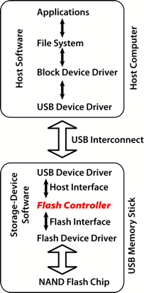
Applications running on the host request file services from a file system implementation. The file system performs block operations using a block device driver, which sends block read/write requests through a USB channel to the USB memory stick. A USB device driver on the USB memory stick receives the requests from the host and forwards them to a piece of software called a flash controller. The flash controller finds the requested block on the flash chip and sends it back, or it receives a block and stores it on flash. The communication with the flash chip is performed by a thin layer of software called the flash device driver, which essentially exposes the capability of the flash chip to the flash controller software.
The goal of this project is to design the flash controller (the red software component in the first diagram above), which is a non-trivial piece of software. The controller will provide a disk-like API that the USB device driver will call. The controller will access the NAND chip through the API of the flash device driver. The complexity of the flash controller results from the fact that its role is to make the flash look like a magnetic disk drive, even though the physical characteristics of flash chips are very different from those of disk drives.
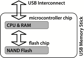
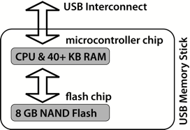
All the software on the USB memory stick runs on a small microcontroller (a chip containing a CPU, a small amount of RAM, and communication channels to the outside world), as shown in the next diagram.
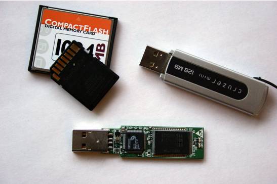
Physically, a USB memory stick looks like the two in the picture below, one without the plastic enclosure and one with an enclosure (the picture also shows a Compact Flash and SD memory cards). In the exposed device, the small square chip is the microcontroller, and the large rectangular one is a flash chip.
These devices use a semiconductor technology called NAND flash to store data on a piece of silicon. Flash is a non-volatile storage medium, which means that the data is retained even when the chip is not powered (using charge trapped on floating gates, which are electrically-insulated parts of each memory cell).
The Flash Device Driver's Interface
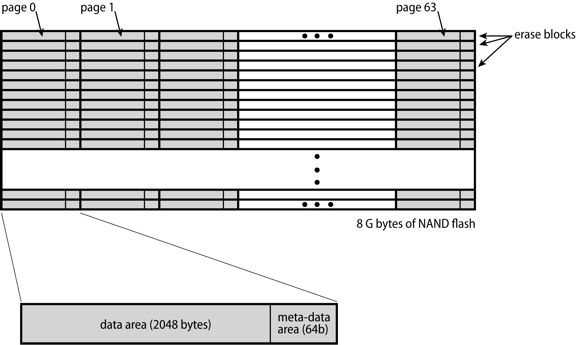
The flash chip that we will use in this project consists of 222 pages (about 4 million). Each page contains two storage areas: a 2048-byte data area, and a 64-byte meta-data area. The software of the flash controller can use the meta-data area for its own use. Pages are grouped into contiguous blocks of 64 pages called erase blocks. When software erases a block, all the bits in the block become ‘1’; the previous contents of the block are lost. This is the only way to set bits in flash. To clear bits (change them from ‘1’ to ‘0’), you write to a page. Once the software writes to a byte, the byte cannot be overwritten until the block that contains it is erased. There are some additional constraints on writing, which are described below. The following diagram shows this structure.
The API of the flash device driver is as follows:
-
void flash_erase(int starting_page_number);
Erases a block of 64 pages, starting at a given page number. The argument must be divisible by 64. This operation takes 2 ms. -
void flash_read(void* buffer, int page_number, int starting_byte,
int length);
Fills the buffer with the data stored in the given flash page, starting from a given byte offset. To ensure that the bytes read are indeed part of the page, the arguments must satisfy the constraints 0 ≤ starting_byte, starting_byte+length ≤ 2111 and length > 0. This operation takes 0.02 ms. -
void flash_write(void* buffer, int page_number, int
starting_byte, int length);
Stores data in the flash. This operation takes 0.2 ms, and is subject to a number of constraints:
o The arguments starting_byte and length must satisfy the same constraints as in flash_read().
o The bytes in this range must not have been written since the page was erased.
o It is only possible to write once to the data area of a page (its first 2048 bytes) between erasures.
o It is only possible to write four times to the meta-data area of a page (its last 64 bytes) between erasures.
The Host Interface
The host views the flash device as an array of 2048-byte sectors. The host reads and writes entire sectors. It can read and write them in any order. This is the interface that magnetic disk drives provide to the host, and our flash storage device emulates a disk. We use the word sector to distinguish the partitioning of the host’s disk-like address space from the partitioning of the flash chip into erase blocks and pages. Note that when a flash page stored the contents of a sector, 64 bytes of the page are still available for the flash controller’s data structures.
The host can invoke the following functions of the flash controller:
-
void format();
The host calls format() to initialize the USB memory stick and prepare it for use. It should ignore any data stored in flash or in the memory stick’s RAM. Sectors can have undefined contents after format(). The function should prepare any on-flash data structures, so that init() can be called (see next). Normally, format() runs only once in the entire life time of the memory stick. -
void init();
The host calls init() when the device is attached and powered, if the device has already been formatted, or after format. When this function is called, data structures in the memory stick’s RAM contain no useful information; they must be initialized by init(). -
void finalize();
The host calls finalize() just before the device is turned off. After this function returns, data will lose power and data in the memory stick’s RAM will be lost. -
int size();
Returns the number of 2048-byte sectors that the device can store. This number can be smaller than the number of pages in the chip. -
void read(void* buffer, int sector_number);
Reads a sector. The second argument is between 0 and size()-1. -
void write(void* buffer, int sector_number);
Writes a sector (the old contents of the sector are lost). Same constraint on the sector number.
The goal of this project is to provide a design for these functions.
Wear Leveling
Your design of the host interface’s functions must address a challenge that flash memories pose. Blocks in flash devices wear out after a certain number of erasures. Our chip is guaranteed to be able to erase and re-write each block 100,000 times. Once a block is erased 100,001 times, writing to it may fail, in which case we consider the entire flash storage non-functional.
Ideally, the host should be able to write 100,000 x 222 sectors to our device before it wears out. Your design won’t be able to achieve this ideal; no practical design can. But your design should maximize the life expectancy of the device by employing some kind of wear-leveling strategy. That is, your design should map sectors to pages in a way that leads to all the blocks being erased roughly the same number of times. The behavior that your design should avoid is erasing a few blocks close to 100,000 times while some other blocks have not been erased much at all. If the controller avoids this behavior, the device will last for many writes even if the host writes to the same sectors over and over again.
Expected Workload
The following characterizes the workload seen by your device.
1. format() will be called at most a few times over the life of the device.
2. finalize() and init() will be called several times a day for a few years, every time the laptop suspends (or is shut down) and wakes up.
3. The device will be subject to sequential and random writes and to sequential and random reads.
4. The host may write very frequently to some sectors and less frequently to others.
There is probably no flash-controller design that performs better than all others under all workload conditions; design involves tradeoffs.
The Design Task
You need to design a flash controller; that is, to design the functions of the host interface. The functions of the host interface provide services by making calls to the flash device driver. Your controller should manage the 8 GB flash chip using only 40 KB of (volatile) RAM for its data structures. The system has a bit more RAM for other purposes, but your data structures should fit in 40 KB. You can also store data structures on flash using whole pages and/or the meta-data area of pages. The following diagram shows the specific hardware that your controller runs on.
Here are the issues that you must consider in your design. You do not necessarily have to optimize each one of these metrics; some of them must probably be traded off for others. Describe your analysis of these issues in your project report:
1. The flash chip has 222 pages, but size() must return a number smaller than 222, because during erasures the flash stores only 222−64 pages, and the memory-stick’s controller can store at most 20 more. If your design stores some of its data structures on the data area of pages, or if the controller reserves pages for some other purpose, size() may return a number that is significantly smaller than 222. What does your size() return?
2. How long does init() run (usually and in the worst case)?
3. What is the performance of sequential writes (writing a sequence of contiguous sectors)? Writes to randomly-selected sectors? Sequential and random reads? Assess performance in terms of the number and timing of flash operations, not in terms of CPU operations. The CPU is sufficiently fast so as not to represent a performance concern unless you use terribly inefficient algorithms (which you should not).
4. How effective is your wear leveling? The design should avoid wearing out some blocks while others have not been erased much.
There are also several issues that real designs must cope with, but that your design should ignore. You will not get any additional credit for a design that deals with these issues or for analysis of them.
1. Dealing with so-called bad blocks, which are blocks that are marked as non-functional by the manufacturer or that fail later (perhaps due to wear). Assume that all the blocks are functional. (In reality, NAND flash chips are shipped with bad blocks marked as such.)
2. Designing init() so that it functions correctly (and reasonably quickly) even after the controller loses power before finalize() is called, or even in the middle of an operation. You can assume that the system is powered off only after finalize() returns.
3. Making the design usable in slightly different flash storage devices. The parameters that we have specified are fairly typical, but individual storage devices are obviously not all identical. Some have more or less RAM. Some flash chips are smaller than 8 GB; some use pages with 512+16-byte pages; some can only endure 10,000 erasures; and so on. But your design should be analyzed only in terms of the hardware that we specified here.
How to Come Up with a Good Design
There is no recipe for coming up with a good design, but there are some techniques that often help.
Start by inventing some design that seems to work. Do not try to figure out whether it is efficient, or optimal. Just convince yourself that it works. Get to the point where you believe that it works and that you’ll be able to fill in all the details if you need to. Then stop thinking about it. If you keep on working on this first design, fleshing out the details or analyzing its performance, you may fall in love with it, even though it may be a pretty bad design. Explore a bit more before you settle down.
Now try to invent another design. Same rules, but try to make it as different as possible from the first one. Do not invent a variation on the first design; invent something radically different. Also stop when you feel confident that it can work; don’t work out the details.
If you can think of yet another design, radically different than the first two, that’s good. But if nothing comes to mind, stay with two.
Now try to understand the differences between the behaviors of the different designs. One will be more efficient in one metric but less efficient in another metric. The different designs help you explore the design space (the range of possible designs), and comparing them helps you understand the inherent (or apparent) tradeoffs in that space.
Pick the design that seems best. Flesh it out and analyze its behavior. Perhaps you can combine ideas from more than one preliminary design in your final design. In your project report, do not discuss discarded designs; spend your energy presenting your final design and justifying it. But do not assume (and do not imply in your report) that your design is the only one possible, or even the only plausible one. Do explain fundamental tradeoffs that you discovered.
We gave you a real-world challenge, so there are obviously real-world solutions to it; some of them might be described in technical papers, or patents, or web pages (but some, perhaps the best ones, might be proprietary trade secrets). If you search, you will find them. Designs of related systems, like file systems, may also contain useful ideas. Learning from other people’s experience is an important design tool (but also use your own creativity!). If you adopt ideas developed by others, cite your sources.
Your Written Work
You will submit two written documents, on different due dates: a proposal and a report.
The proposal should be written as a memo to your boss. It should describe the data structures that the flash controller will use, and it should analyze its performance in one access-pattern case (random or sequential, read or write). The goal of the proposal is to help your boss (in reality the 6.033 staff) assess whether you are in the right direction and to provide you with feedback accordingly. You will receive this feedback on it on time to adjust your final report.
Your design report should be written for two persons: a fellow designer, who will review and evaluate the design before it is implemented, and a programmer who will implement it afterwards. Assume that will have read the assignment before reading your report. Use the following structure for the report (the proposal consists of the high-level design section and an analysis plan):
- Title page: Give your design report a title that reflects the subject and scope of your project. Include your name, recitation time and section, and the date on the title page.
- No Table of Contents.
- Introduction. A brief overview of your approach and design goals. This shouldn't be a detailed description, but rather a high-level overview to provide the reader with sufficient context for the details in subsequent sections.
- Data Structures. Explain the abstractions that you use and the main idea behind them and their implementation. Describe the data structures that the flash controller uses, both in the memory-stick’s RAM and on flash. Use both text and diagrams to explain the data structures. If a diagram shows an example, make it detailed enough that it explains the design but not too detailed. Explain the diagram itself in its caption or in the text. But remember to also describe the data structures in the text.
- Algorithms: Describe how each of the flash-controller’s function works. The algorithms must be described in the text. Diagrams help here too (before/after diagram or step-by-step diagrams showing how a data structure changes are appropriate for explaining algorithms). Pseudo-code may also help, but not if it is too long, too detailed, or ambiguous.
- Analysis: Present your analysis of the design (the list of issues to be analyzed appears above). Analyze quantitatively whenever possible. Explain the tradeoffs you made and provide a rationale for the design that you have chosen. If you made any assumptions apart from those in the assignment, state them explicitly.
- Summary: Summarize what the design achieves, top-level tradeoffs, and what issues remain to be addressed, if any.
- Acknowledgements and References: Give credit to individuals whom you consulted in developing your design. Reference any sources cited in your report (and obviously cite sources that you have used). The style of your references should be in the format described in the Mayfield Handbook's explanation of the IEEE style.
How do we evaluate your report?
When evaluating your report, your recitation instructor will look at both content and writing and assign a letter grade. The writing program will grade the report separately for writing and assign a letter grade.
The recitation instructor will assign approximately 30% of the grade to the data structures, 30% to the algorithms, and 40% to the analysis.
We assess each one of these components according to the following criteria. The criteria are listed in order of importance.
- Clarity. Is the design described well enough to be evaluated and implemented? Can the reader understand your analysis? If we cannot understand your design and analysis, we cannot fully assess the other criteria.
- Correctness and completeness.
- Simplicity. How complex is your solution? Simple is better, yet sometimes simple will not do the job. On the other hand, unnecessary complexity is bad.
- Performance (of the flash controller). This criterion pertains only to the data structure and algorithms sections, not to the analysis section.
Some writing considerations:
- Is the report well-organized? Does it follow standard organizational conventions for technical reports? Are the grammar and language sound?
- Do you use diagrams and/or figures appropriately? Are diagrams or figures appropriately labeled, referenced, and discussed in the text?
- Does the report use the concepts, models, and terminology introduced in 6.033? If not, does it have a good reason for using different vocabulary? In particular, use the terminology that the textbook uses; the Glossary sections are particularly helpful.
- If you introduce specialized terminology, is it clear and is it used consistently? In the text of this assignment we introduced the terms page, erase block, and sector. They all refer to blocks of memory, but if we used the term “block” for all of them, the text would have been very confusing.
- Does the report address the intended audience?
- Are references cited and used correctly?
Collaboration
This project is an individual effort. You are welcome to discuss the problem and ideas for solutions with your friends, but if you include any of their ideas in your solution you should explicitly give them credit. You must be the sole author of your report.
Last updated: $Date: 2008-03-15 00:58:16 -0400 (Sat, 15 Mar 2008) $