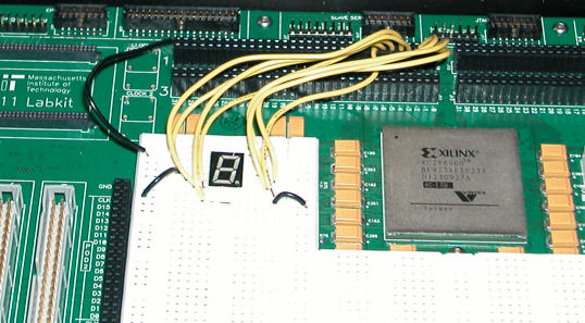
Add Verilog code to the labkit module using four of the
labkit's slide switches to specify which hex digit to display on a
7-segment display. The switch port of the labkit module is
an 8-bit value reflecting the current settings of the labkit's slide
switches. Use switch[3:0] as the 4-bit hex digit to be
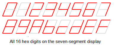
displayed. Here's the appropriate pattern of segments for each
digit:
Compute the appropriate value for each of segment control signals
and drive them onto the appropriate FPGA output pins (I used
user1[7:0]). (There are two rows of pins. Be sure to use
the signal pins and not the grounds.) Note that you'll have to modify
or comment-out the existing line in the code that sets a default value
for the output pins you're using.
Synthesize and implement your design. Generate a programming file
and configure the FPGA. When your circuit is working, you should
be able to display 0-f on the 7-segment display using the switches.
Unless you following the instructions exactly, you synthesis will
fail - labkit.ucf file includes constraints for all of the input
and output ports defined in labkit.v. Most designs, however, will not
use all of these signals, in which case the synthesis engine will
optimize the unused signals out of the design. The location
constraints in labkit.ucf for these unused signals will then generate
errors. It is therefore necessary to tell ISE not to generate an
error if it encounters a pin constraint for a (now) nonexistent
signal. To do this, right-click on the "Implement Design" item in the
process pane, and select "Properties...". Check the box to "allow
unmatched LOC constraints" in the "Translate Properties" form.
Add Verilog to your module by replacing 4 slide switches with the
output of a 4 bit counter. Increment the count on every rising edge of
button_enter.
	//////////////////////////////////////////////
	//
        always @(posedge button_enter)
        counter<=counter+1;
	//
        // using the edge of an external input as a
        // clock is poor design practice!
	/////////////////////////////////////////////
Because of switch bounce, the counter may increment by more than one.
Switch bounce typically disappears after 10-20 ms. One approach to debouncing
is to sample the input. The input is considered valid only if the
value is the same for some period of time. Add Verilog to debounce
the switch input so that each press of button_enter increments the
count by one. For debouncer, a signal is considered to be clean if
the value remains the same for 10msec. With a 27mhz clock, that's
270,000-1 clock cycles.
Step 1: At each clock pulse, store the new input into a reg
Step 2: if the new input is the same as the previous input, increment a counter. If not
it must be switch bounce so set
the counter to zero. When the counter reaches 270,000-1, you have a debounced input.
Here's a skelton of the debounce Verilog:
	//////////////////////////////////////////////
	//
        module debounce(
            input clk,       // check the name of your clock
            input reset,     // system reset
            input bouncey_input,
            output reg clean_data
            );
           reg [18:0] count; // is 19 bits enough?
           reg old;
           always @(posedge clk) begin

             ... your Verilog

                end

        endmodule
	//
	/////////////////////////////////////////////
When your circuit is working, ask a staff member to
check you off. (1.1 point) For checkoff be prepared to show your
circuit in operation, incrementing the count with each button_enter
press.