Figure 1
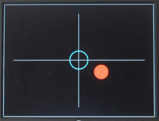
Goal: Design a digital bubble level using data from an inertial measurement unit (IMU) and display the results on a monitor. When the IMU is lying flat on a surface parallel to the ground, the bubble will be centered in the circle. (This lab was inspired by the Virtual Softball project by Katie Shade and Melinda Szabo F2017.) This lab provides you with a design methodology that will be useful in your final project.
Figure 1
Useful links
Checkoff List
Please have the following available during checkoff:
Be able to respond to any of the following questions (and possibly others).
[Checkoff: 4 points, 5 points with added features - see end]
Digital Bubble Level
In this lab you will implement a digital bubble level using serial data from an MPU-9250 IMU. The MPU-9250 is a multi-chip module consisting of a 3-Axis gyroscope, the 3-Axis accelerometer and 3-Axis magnetometer. For this lab we will use only the accelerometer data for x,y axis. [Note: the Nexys4 includes Analog Device ADXL362 accelerometer with a SPI interface. However, the experience of attaching and using peripherals devices may come in handy during the project phase.] The accelerometer measures acceleration forces in three axes. These forces may be static such as gravity or dynamic such as motion or vibration. A common application is display rotation when smart phone display is rotated.
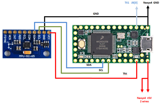
IMU data for all three axes is sent via I 2 C bus with clock (SCL) and data (SDA) lines to a Teensy, then packetized and transmitted by an universal asynchronous receiver-transmitter (UART) to an I/O pin at 9600 baud. (See Lab 2 for a refresher on serial data. In Lab 2, a transmitter was implemented. For this lab the goal is to a design receiver.)
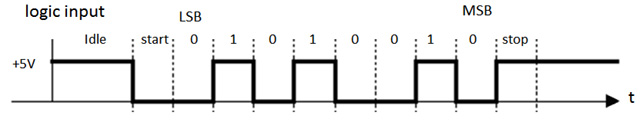
The data is 6 bytes (16 bits for each axis) for x,y,z data respectively with the least significant bit of the least significant byte first. The data for each axis is in 2's complement format.
The x,y coordiates are then used as inputs to move a circle with 0,0 the center of screen.
Procedure
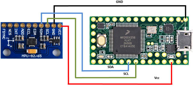
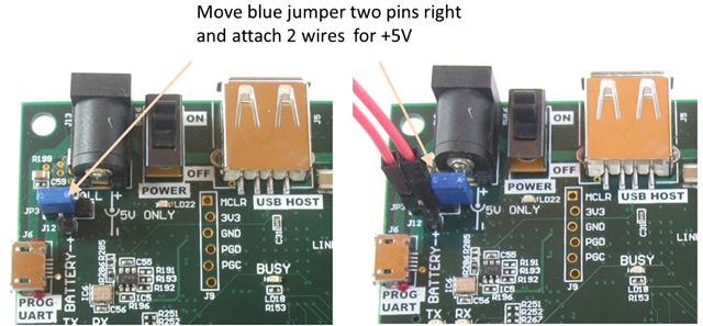
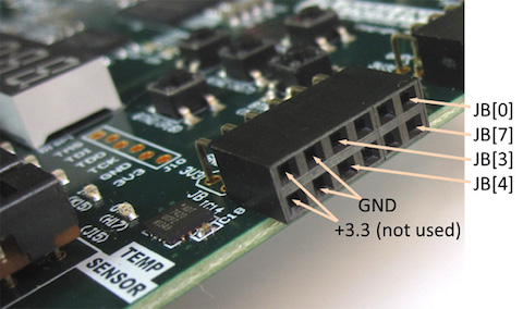
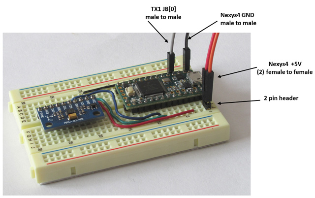
It is general practice to use black wire for ground and red wire
for Vcc. There are colored wires near the center columns of the lab.
Make a quick check to verify everything is working correctly by
attaching a spare USB cable (available at the TA station) to Teensy
and any computer. The board, if wired correctly, will act as a tilt
sensitive mouse.
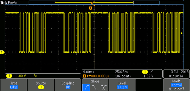
Data is sampled at 100 Hz and sent at 9600 baud (104us for each data bit) with approximately a 4ms interval betweent sets. The bits are as follows:
Implementation Suggestions
Your clocked state machine has an asynchronous input, potentially creating a problem with metastability in the state registers if the input changes too near a rising clock edge. In general asynchronous inputs need to be synchronized to the internal clock before they can be used by the internal logic. synchronize.v (included in the labkit_lab5c.v) is a Verilog implementation of a pulse synchronizer that can convert an asynchronous signal to a synchronous one with acceptably low probability of metastability in the synchronous signal.
The labkit template module does not have a reset signal. It may be useful to implement a reset signal using a button/switch input. Be sure to debounce the signal.
Since the incoming signal is asynchronous, sampling at 16x is needed at receiving to ensure that the input data stream is correctly sampled with respect to the falling edge of the start bit. This was not necessary when transmitting but is crucial when receiving.
Look for 1 → 0 transition for the beginning of start bit. If sampling at 16x, the middle of the start bit should be 8 sampling clocks from the falling edge. Each subsequenty data bit can then be sampled every 16 sampling clocks. Check format (start, data, parity, stop bits) before accepting data.
At 9600 baud, each bit is 104us. Check and see that the data line is high for at least 2ms before looking for the first start bit. This will ensue that the FSM does not start in the middle of a data stream. When the start bit is detected, begin capturing the data bits.
One approach, thinking as a programmer is to store each byte as the bits arrive. This requires keeping track of the number of bits arriving and storing the data appropriately. A top MIT engineer would treat the incoming data as a 60 bit data stream, shift 60 bits in, pull the x, y values from the 60 bits and store the x, y values in 16 bit registers. [When solving a problem, consider alternative designs - look for an elegant or simplier solution.]
Display the x, y accleration using 4 digits for each axis - converting from 2's complement to plus/minus format. For each axis, use the most significant 13 bits. Since the hex display cannot display a minus sign, display a "F" insstead. The value 1 [0_0000_0000_0001] will display 0001. The value -1 [1_1111_1111_1111] display as F001.
Use SW[15] for calibration. With board lying flat and SW[15]=0, the display shows the actual x,y accelerator values. With SW[15]=1, an offset to x,y is added so the hex display shows 0,0 and the circle is centered at the cross hairs. Using the calibrated values, SW[15]=1, offset the bubble appropriately. To demonstrate that calibration is working correctly, tilt the IMU and calibrate that orientation as "flat".
Create a 64 pixel diameter circle (bubble). Drawing a circle is similar to drawing a rectangular blob except it uses the circle equation x 2 + y 2 ≤ r 2 to determine the color of the pixel. Depending on speed of the multipliers, pipelining may be necessary in generating a circle. Use the x,y values to move the center of the circle with 0,0 at the cross hairs. Now draw a ring surrounding the circle to create the display shown in figure 1.
Check off
Display cross hairs with bubble[4 points]. Be able to demonstrate all of the following:
Earn an additional point by:
Labkit_lab5c.v
The labkit_lab5c.v template top-level file and others files can be downloaded from the links at the beginning of this document.
Compile and load the project to the Nexys4. SW[1] will toggle between color bars and cross hairs display. The graphics are 1024x768 with a 65Mhz clock. (If white borders are not aligned, press the auto-adjust button next to the Power button on the display.) You are free to modify the display in any manner in completing the lab. Note: the Nexys4 has 12 bit VGA compared to 24 bit for the labkit. Design accordingly.
It's good design practice to use one clock domain - so use 65Mhz as your system clock. The Verilog files allow a user to utilize some of the Nexys 4 features including buttons, switches, LEDs, user input/output pins, VGA output, etc.
You will need to instantiate all submodules in this top level file as well as create wires to connect the submodules.
In addition, you will need to connect the input that you use to the appropriate submodules. There are Verilog statements in labkit_lab5c.v that set default values for outputs: the LEDs, 7 segment... You'll need to replace those statements with your own logic.
Debugging
Inevitably your design won't be 100% correct the first time. Debugging by just observing the hex display may not be of any use - you'll need more info to figure out what's happening. Start by building a test-jig for each module of your design and then run simulation to verify the expected behavior of the system on several sequences of inputs. This will eliminate many of the problems. To wring the tricky problems use the integrate logic analzer (ILA). The display will give you real time debugging information.