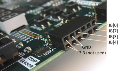
Figure 1
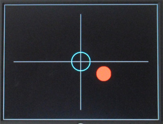
Goal: Design a digital buble level using data from an inertial measurment unit (IMU) and display the results on a monitor. When the IMU is lying flat on a surface parallel to the ground, the bubble will be centered in the circle. (This lab was inspired by the Virtual Softball project by Katie Shade and Melinda Szabo F2017.) This lab provides you with a design methodology that will be useful in your final project.
Figure 1
Checkoff List
Please have the following available during checkoff:
Be able to respond to any of the following questions (and possibly others).
[Checkoff: 4 points, 5 points with added features - see end]
Digital Bubble Level
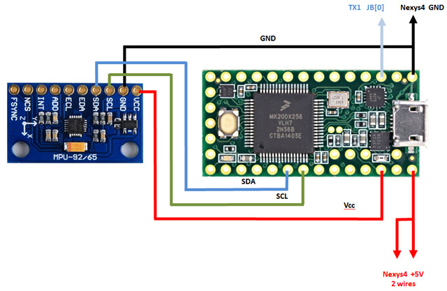
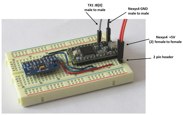
In this lab you will implement a digital bubble level using serial data from an MPU-9250 IMU. The MPU-9250 is a multi-chip module consisting of a 3-Axis gyroscope, the 3-Axis accelerometer and 3-Axis magnetometer. For this lab we will use only the accelerometer data for x,y axis. [Note: the Nexys4 includes Analog Device ADXL362 accelerometer with a SPI interface. However, the experience of attaching and using peripherals devices may come in handable during the project phase.] The accelerameter measures acceleration forces in three axis. These forces may be static such as gravity or dynamic such as motion or vibration. A common application is display rotation when smart phone display is rotated.
IMU data for all three axis is sent via I 2 C bus with clock (SCL) and data (SDA) lines to a Teensy, then packetized and transmitted by an universal asynchronous receiver-transmitter (UART) to an I/O pin at 9600 baud. (See Lab 2 for a refresher on serial data.)
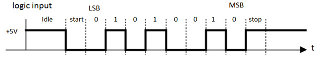
The data is 6 bytes (16 bits for each axis) for x,y,z data respectively with the least significant bit of the least significant byte first. The data for each axis is in 2 complement format.
The x,y coordiates are then used as inputs to move a circle with 0,0 the center of screen.
To make things more complicated, the Ethernet protocol while it uses little endian at the bit level, uses big endian at the byte level! So, a 16-bit value with bits being labeled 0 to 15 for lsb to msb, respectively, is transmitted with Ethernet as bit order: 8-9-10-11-12-13-14-15 - 0-1-2-3-4-5-6-7. See IEEE 802.3 Clauses 3.1.1, 3.2.6, and 3.3 for the gruesome details.
For this lab, the data sent on the I2C bus is big endian (msb first) but bit banged [converted] to little endian to comply with the RS-232 protocol. To be safe, always check the datasheet for bit and byte ordering.
Procedure
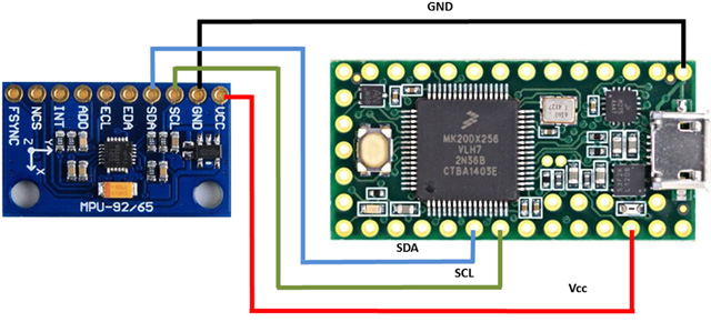
It is general practice to use black wire for ground and red wire
for Vcc. There are colored wires near the center columns of the lab.
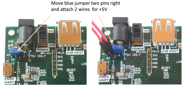
Make a quick check to verify everything is working correctly by
attaching a spare USB cable (availabe at the TA station) to Teensy
and any computer. The board, if wired correctly, will act as a tilt
sensitive mouse.
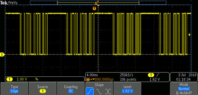
Data is sampled at 100 Hz and sent at 9600 baud (104us for each data bit) with approximately a 4ms interval betweent sets. The bits are as follows:
Implementation Suggestions
You may use the pong game starter files for this lab. The xdc files will need to be modified accordingly for the IMU inputs.
Your clocked state machine is uses a asynchronous input, potentially creating a problem with metastability in the state registers if the input changes too near a rising clock edge. In general asynchronous inputs need to be synchronized to the internal clock before they can be used by the internal logic. synchronize.v (from previous labs) is a Verilog implementation of a pulse synchronizer that can convert an asynchronous signal to a synchronous one with acceptably low probability of metastability in the synchronous signal.
It may be useful to implement a reset signal using a button/switch input. Be sure to debounce the signal.
Since the incoming signal is asynchronous, sampling at 16x is needed at receiving to ensure that the input data stream is correctly sampled and valid bits are read. This was not necessary when transmitting but is crucial when receiving.
Look for 1 → 0 transition for the beginning of start bit by sampling the incoming data. If sampling at 16x, the middle of the start bit should be 8 sampling clocks from the falling edge. Each subsequenty data bit can then be sampled every 16 sampling clocks. Check format (start, data, parity, stop bits) before accepting data.
At 9600 baud, each bit is 104us. Check and see that the data line is high for at least 2ms before looking for the first start bit. This will ensue that the FSM does not start in the middle of a data stream. When the start bit is detected, begin capturing the data bits.
One approach for this lab, is to store each byte as the bits arrive. This requires keeping track of the number of bits arriving and storing the data appropriately. Another approach thinking as a hardware enginer engineer would treat the incoming data as a 60 bit data stream, shift 60 bits in, pull the x, y values from the 60 bits and store the x, y values in 16 bit registers. [When solving a problem, consider alternative designs - look for an elegant or simplier solution.]
Display the x, y accleration using 4 digits for each axis - converting from 2's complement to plus/minus format in hex with the most significant digit displaying the sign. For each axis, use the most significant 13 bits. Modify the hex display to display a minus sign. For positive values turn all the segments off for the sign digit. The value 1 [0_0000_0000_0001] will display _001. The value -1 [1_1111_1111_1111] will display as -001. With the IMU laying flat, the display should show 0,0 and increase/decrease as the IMU is tilted. This shows you have successfully read in the IMU data.
Use sw[15] for calibration. With board lying slightly tilted and sw[15]=0, the display shows the actual x,y acceleration values. With the board in the same position and sw[15]=1, an offset to x,y is added so the hex display shows 0,0 and the circle is centered at the cross hairs. Demonstrate that calibration is working correctly by tilting the IMU and calibrate that orientation as "flat".
Create a 64 pixel diameter circle (bubble). Drawing a circle is similar to drawing a rectangular blob except it uses the circle equation x 2 + y 2 ≤ r 2 to determine the color of the pixel. Each multiply has a 4ns propagation delay. Pipelining may be necessary in generating a circle.
A better approach is to implement a single pole low pass IIR
(Infinite Impulse Response) filter where past samples with a decay
factor d, are taken into account.
y[n] = (1-d)x[n] + dy[n-1] with d < 1
The filter is an IIR since for 0 < d < 1, y[n] depends upon all past samples.
Qualitatively, as d approaches zero, y[n] responds instantaneously to x[n], i.e. higher frequency response. As d increases, pass samples have a greater impact thus slowing the response. The cutoff frequency, fc, is defined as the frequency where the power is one half of the input. For the single pole IIR filter, fc = -ln(d)/2π. [If this topic is interesting, consider 6.341, Discrete Time Signal Processing.] This is the digital equivalent of a RC filter with a fc = 1/(2πRC)
For the lab, implement a IIR filter where the decay factor is determine by d = sw[14:11]/16. At check off demonstrate operation for various values of d. Be very careful in implementing the math. The order of operation has a great bearing on the precision of the calculation. Using 8 bit math, with a starting value of n=4, y=(n/16)*16 = 0, while z = (n*16)/16 = 4. That's the difference between digital logic and programming.
Check off (5 total points)
Display cross hairs with bubble[4 points]. Be able to demonstrate all of the following:
Earn an additional point by adding an interesting/fun feature. Really good ones may be included in future terms.
Suggestions and Debugging
It's generally a good idea to implement the lab in subsystem blocks. For this lab, the possible blocks are sampling the incoming data, moving the bubble and IIR filter.
Inevitably your design won't be 100% correct the first time. Debugging by just observing the hex display may not be of any use - you'll need more info to figure out what's happening. Start by building a test-jig for each module of your design and then run simulation to verify the expected behavior of the system on several sequences of inputs. This will eliminate many of the problems. For really tough problems use the integrate logic analzer (ILA). The display will give you real time debugging information.