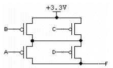
 What is the correct schematic for the pullup
circuitry?
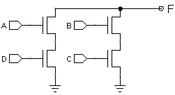
What is the correct schematic for the pullup
circuitry?
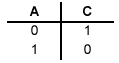
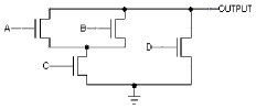
 Assuming the pullup circuitry is designed correctly, what is
the logic function implemented this gate?
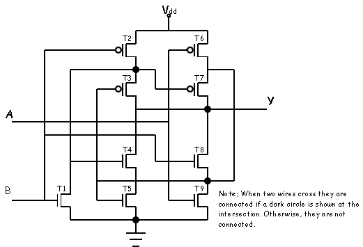
Assuming the pullup circuitry is designed
correctly, when the output of the CMOS gate above
is a logic "0", in the steady state what would we
expect the voltage of the output terminal to be?
What would be the voltage if the output were a
logic "1"?
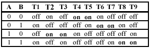
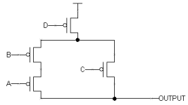
Assuming the pullup circuitry is designed correctly, what is
the logic function implemented this gate?
Assuming the pullup circuitry is designed
correctly, when the output of the CMOS gate above
is a logic "0", in the steady state what would we
expect the voltage of the output terminal to be?
What would be the voltage if the output were a
logic "1"?