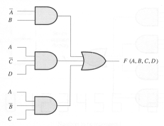
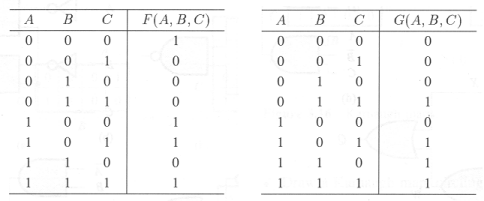
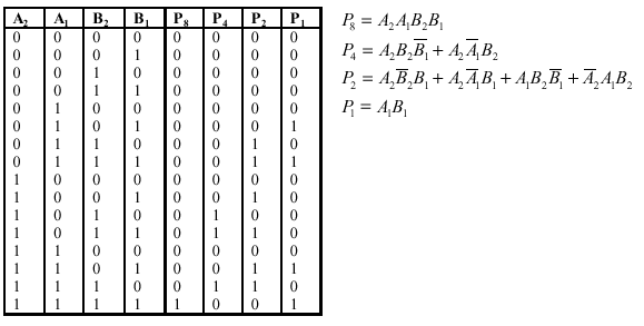
We can construct a sum-of-products expression from a truth table
by writing down a product term for each line of the table where
the output is 1. Each product term contains all the input
variables: directly (ie, "A") if that variable is 1 for this
line of the truth table, or negated (ie, "not A") if that variable
is 0 for this line of the truth table. We then OR the product terms
together to get the final expression:
           _ _ _     _ _     _
F(A,B,C) = A*B*C + A*B*C + A*B*C + A*B*C
           _         _         _
G(A,B,C) = A*B*C + A*B*C + A*B*C + A*B*C
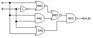
 Fill in the following truth table for H:
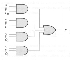 What are the values of C0 through C3
that would cause F to be the exclusive OR
of A and B?
What are the values of C0 through C3
that would cause F to be the exclusive OR
of A and B?
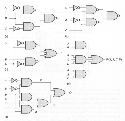
 Waveforms with lenient gates:
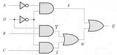
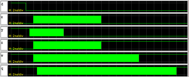
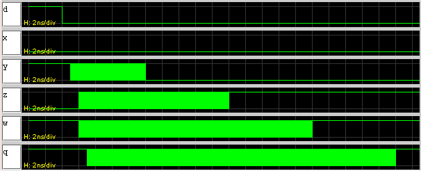 where we see that X doesn't change since the value of A
is sufficient to determine the value of X.
where we see that X doesn't change since the value of A
is sufficient to determine the value of X.
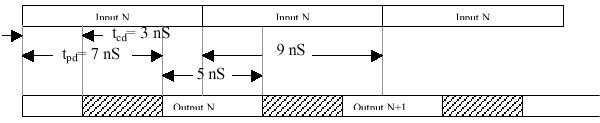
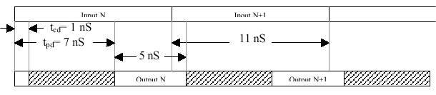 Thus if the inputs transition no faster than every 11ns (~90 MHz),
the outputs will be stable for at least 5ns.
Thus if the inputs transition no faster than every 11ns (~90 MHz),
the outputs will be stable for at least 5ns.

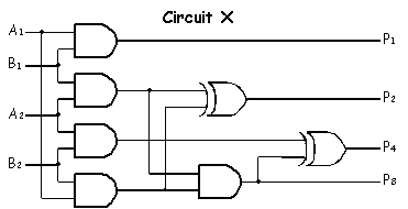
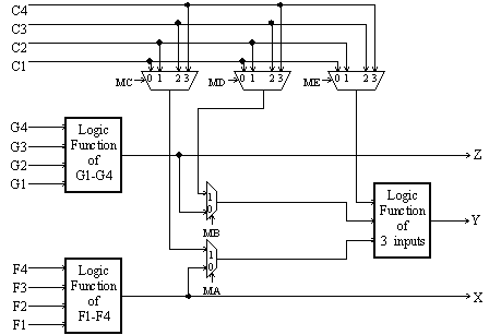 There are two 4-input function generators and one 3-input function
generator, each capable of implementing an arbitrary Boolean function
of its inputs.
The function generators are actually small 16-by-1 and 8-by-1
memories that are used as lookup tables; when the Xilinx device is
"programmed" these memories are filled with the appropriate values so
that each generator produces the desired outputs. The multiplexer
select signals (labeled "Mx" in the diagram) are also set by the
programming process to configure the CLB. After programming, these Mx
signals remain constant during CLB operation.
The following is a list of the possible configurations. For each
configuration indicate how each the control signals should be
programmed, which of the input lines (C1-C4, F1-F4, and G1-G4) are
used, and what output lines (X, Y, or Z) the result(s) appear on.
There are two 4-input function generators and one 3-input function
generator, each capable of implementing an arbitrary Boolean function
of its inputs.
The function generators are actually small 16-by-1 and 8-by-1
memories that are used as lookup tables; when the Xilinx device is
"programmed" these memories are filled with the appropriate values so
that each generator produces the desired outputs. The multiplexer
select signals (labeled "Mx" in the diagram) are also set by the
programming process to configure the CLB. After programming, these Mx
signals remain constant during CLB operation.
The following is a list of the possible configurations. For each
configuration indicate how each the control signals should be
programmed, which of the input lines (C1-C4, F1-F4, and G1-G4) are
used, and what output lines (X, Y, or Z) the result(s) appear on.