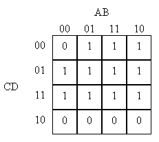
A  B  C | F
========|===
0  0  0 | 1
0  0  1 | 0
0  1  0 | 0
0  1  1 | 1
1  0  0 | 1
1  0  1 | 1
1  1  0 | 0
1  1  1 | 1
 Write a sum-of-products expression for F.
    _ _ _   _         _ _     _
F = A*B*C + A*B*C + A*B*C + A*B*C + A*B*C
Write a minimal sum-of-products expression for F.
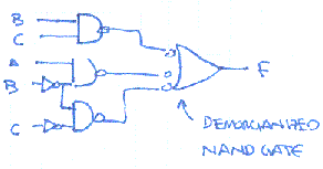
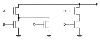
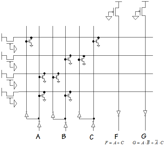
Show a combinational circuit that implements F using only
INV and NAND gates.
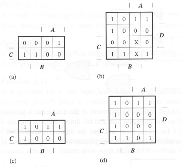
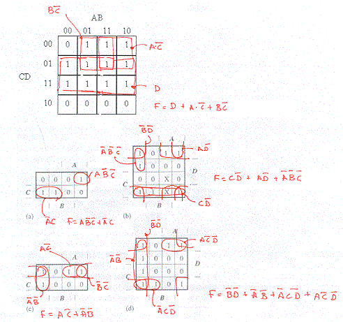
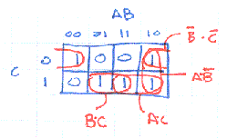 To cover all the 1's in the map we have to use 3 of the 4 patches:
    _ _     _
F = B*C + A*B + B*C
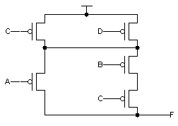
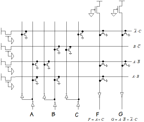
One possible schematic diagram is shown below. Note that
the final 3-input NAND gate has been drawn in it's Demorganized
form, i.e., an OR gate with inverting inputs.
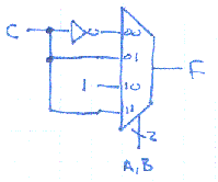
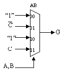
 Implement F using one 4-input MUX and inverter.
 Write a minimal sum-of-products expression for NOT(F).
      _   _ _
F = B*C + A*B*C
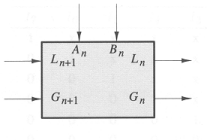 The inputs are labeled An, Bn, Gn+1, and Ln+1, and the outputs are
labeled Gn and Ln. The G and L signals have the meanings "A greater
than B" and "A less than B," respectively. If both G and L are false,
the meaning is A = B. G and L are never both true. Two k-bit numbers
A and B may be compared using a circuit such as the following:
The inputs are labeled An, Bn, Gn+1, and Ln+1, and the outputs are
labeled Gn and Ln. The G and L signals have the meanings "A greater
than B" and "A less than B," respectively. If both G and L are false,
the meaning is A = B. G and L are never both true. Two k-bit numbers
A and B may be compared using a circuit such as the following:
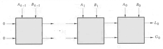 The most significant bits are supplied as Ak-1 and
Bk-1, and the least significant bits are A0 and B0.
The output of a comparison is taken from the G and L outputs of the
lowest-order cell (G0 and L0). Gn+1 and Ln+1 of the highest-order
cell are connected to logical 0 to indicate that the numbers are
assumed to be equal until some difference is found between a pair of
bits Ai and Bi.
If the Gn+1 and Ln+1 inputs indicate that higher-order bits have
established A > B or A < B, then cell n must propagate that
result to Gn and Ln. However, if Gn+1 and Ln+1 indicate that the
higher-order bits are equal, then cell n must compare its bit of A and
B to determine if A > B, A < B, or A = B and must signal that
result appropriately at Gn and Ln.
The most significant bits are supplied as Ak-1 and
Bk-1, and the least significant bits are A0 and B0.
The output of a comparison is taken from the G and L outputs of the
lowest-order cell (G0 and L0). Gn+1 and Ln+1 of the highest-order
cell are connected to logical 0 to indicate that the numbers are
assumed to be equal until some difference is found between a pair of
bits Ai and Bi.
If the Gn+1 and Ln+1 inputs indicate that higher-order bits have
established A > B or A < B, then cell n must propagate that
result to Gn and Ln. However, if Gn+1 and Ln+1 indicate that the
higher-order bits are equal, then cell n must compare its bit of A and
B to determine if A > B, A < B, or A = B and must signal that
result appropriately at Gn and Ln.
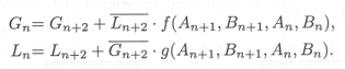
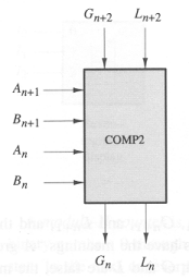 Work out expressions for Gn and Ln as functions of Gn+2, Ln+2,
An+1, Bn+1, An, and Bn. Express your answers in the form
Work out expressions for Gn and Ln as functions of Gn+2, Ln+2,
An+1, Bn+1, An, and Bn. Express your answers in the form