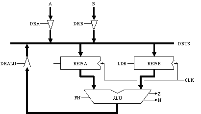
 The heavy lines represent busses, which are many signals grouped
together, e.g., an eight-bit bus is eight separate signal wires that
are treated as a group. When a bus connects to one or more
components, it's just shorthand for drawing the individual signal
wires between those components.
The heavy lines represent busses, which are many signals grouped
together, e.g., an eight-bit bus is eight separate signal wires that
are treated as a group. When a bus connects to one or more
components, it's just shorthand for drawing the individual signal
wires between those components.
 Draw a schematic showing how a tristate driver might
be implemented using mosfets. Hint: The following schematic shows one
way of implementing a tristate driver.
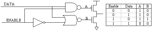
Draw a schematic showing how a tristate driver might
be implemented using mosfets. Hint: The following schematic shows one
way of implementing a tristate driver.
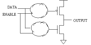 You just have to fill in the logic inside each of the clouds-think
about for what values of DATA, ENABLE you want the pullup to be on and
replace the upper cloud with one or more logic gates that implement
that equation. Ditto for the pulldown and lower cloud.
You just have to fill in the logic inside each of the clouds-think
about for what values of DATA, ENABLE you want the pullup to be on and
replace the upper cloud with one or more logic gates that implement
that equation. Ditto for the pulldown and lower cloud.
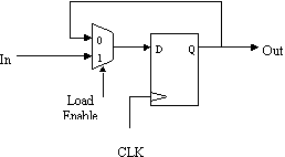
 The register-like symbols labeled "Reg A" and "Reg B" also have an
additional enable input and are called load-enabled registers. When
the enable is high, the register will be loaded from the incoming
data. When the enable is low, the register reloads itself with its
previous value. Show how to implement a load-enabled register from a
regular D-register and a 2-way multiplexer.
The register-like symbols labeled "Reg A" and "Reg B" also have an
additional enable input and are called load-enabled registers. When
the enable is high, the register will be loaded from the incoming
data. When the enable is low, the register reloads itself with its
previous value. Show how to implement a load-enabled register from a
regular D-register and a 2-way multiplexer.
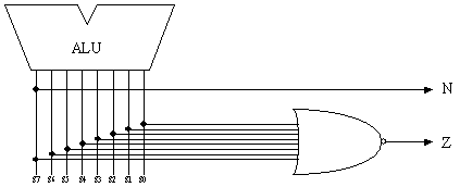
-
when FN = 0, the ALU output is A-B
when FN = 1, the ALU output is B-A
-
Z = 1 when the ALU output is the number "0"
N = 1 when the ALU output is a negative number
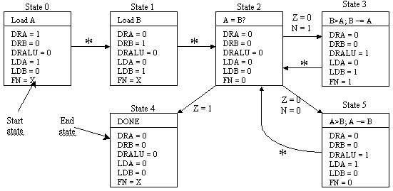
 Your job is to build a controller that will cause the circuit above to
execute the following algorithm which computes the greatest common
divisor of two inputs:
Your job is to build a controller that will cause the circuit above to
execute the following algorithm which computes the greatest common
divisor of two inputs:
	while (a != b)
		if (a > b) a = a - b;
	 	else b = b - a;
The controller will be a state machine that takes 2 bits of input (Z and N) and produces control signals for the data paths (DRA, DRB, DRALU, LDA, LDB, FN). Draw a state diagram for the controller. Outputs from your FSM should depend only on the current state. Indicate which are the initial and final states of your FSM on the diagram.
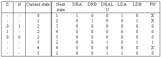
 Supply a truth table for the logic that generates the control signals.
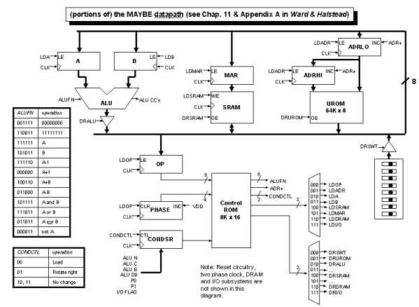 Some features of the MAYBE: