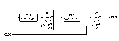
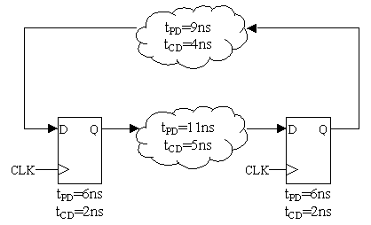
 The components labeled CL1 and CL2 are combinational; R1 and R2 are
edge-triggered flip flops. Timing parameters for each component are
as noted.
The components labeled CL1 and CL2 are combinational; R1 and R2 are
edge-triggered flip flops. Timing parameters for each component are
as noted.
 Write the timing specifications (tS, tH, tCD, tPD, tCLK) for the
system as a whole using the timing specifications for the internal
components that are given in the figure.
Write the timing specifications (tS, tH, tCD, tPD, tCLK) for the
system as a whole using the timing specifications for the internal
components that are given in the figure.
-
tH,R2 <= tCD,R1 + tCD,CL2
2 <= 1 + 1
2 <= 2
-
tS = tPD,CL1 + tS,R1 = 6, and
tH = tH,R1 - tCD,CL1 = 1.
-
tCD = tCD,R2 = 2, and
tPD = tPD,R2 = 8.
-
tCLK >= tPD,R1 + tPD,CL2 + tS,R2
tCLK >= 2 + 5 + 4
tCLK >= 11
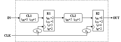
Suppose you had available a faster version of CL2 having a propagation
delay of 3 and a contamination delay of zero. Could you substitute
the faster CL2 for the one shown in the diagram? Explain.
-
tS = tPD,CL1 + tS,R1 - d1 = 6 - d1
tH = tH,R1 - tCD,CL1 + d1 = 1 + d1
tCD = tCD,R2 + d2 = 2 + d2
tPD = tPD,R2 + d2 = 8 + d2
-
tCLK >= tPD,R1 + tPD,CL2 + tS,R2
tCLK >= 2 + d1 + 5 + 4 - d2
tCLK >= 11 + d1 - d2
-
tH,R2 <= tCD,R1 + tCD,logic
2 + d2 <= 1 + d1 + 1
d2 <= d1
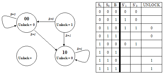
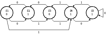
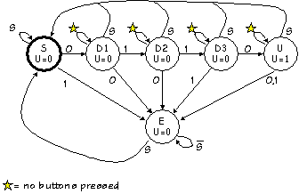 Recall that this design has three buttons labeled "0", "1", and
"Start", and generates an unlock signal U=1 when the user presses
Start followed by the sequence 0,1,1,0.
Unfortunately your partner, Mark Ting, insists that the 6.004
design is way too complex for normal users to understand. After asking
you to help figure out how to make his watch stop beeping ("I never
could figure out how to operate this damned thing"), Mark questions
the need for a Start button. If 0110 is the combination, he argues,
why can't I just walk up and enter 0,1,1,0 and have the lock open?
After some reflection, you conclude that he may have a point.
Recall that this design has three buttons labeled "0", "1", and
"Start", and generates an unlock signal U=1 when the user presses
Start followed by the sequence 0,1,1,0.
Unfortunately your partner, Mark Ting, insists that the 6.004
design is way too complex for normal users to understand. After asking
you to help figure out how to make his watch stop beeping ("I never
could figure out how to operate this damned thing"), Mark questions
the need for a Start button. If 0110 is the combination, he argues,
why can't I just walk up and enter 0,1,1,0 and have the lock open?
After some reflection, you conclude that he may have a point.
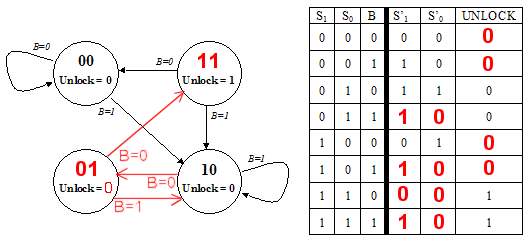
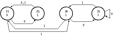
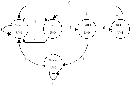 The name of each state represents how many digits in the sequence
have been input. State Sxxxx indicates that the sequences has not begun,
Sxxx0 indicates that the first 0 has been input, etc.
The name of each state represents how many digits in the sequence
have been input. State Sxxxx indicates that the sequences has not begun,
Sxxx0 indicates that the first 0 has been input, etc.
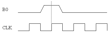
 The button circuitry converts each button press into a single pulse
guaranteed to be stable the required amount of time before and after
the rising edge of the clock. For example, pressing "B0" once
produces the following waveform:
The button circuitry converts each button press into a single pulse
guaranteed to be stable the required amount of time before and after
the rising edge of the clock. For example, pressing "B0" once
produces the following waveform:
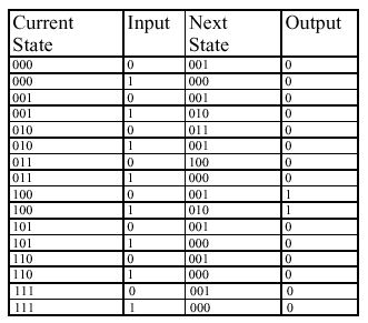
 In answering the questions below, assume that the value of the
UNLOCK output is only a function of the current state.
In answering the questions below, assume that the value of the
UNLOCK output is only a function of the current state.
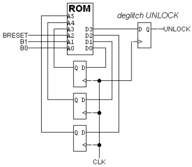
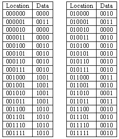 If the lock is programmed with this ROM data, what happens when
"B0" and "B1" are pressed at the same time? Assume that "Breset" is
not pressed.
If the lock is programmed with this ROM data, what happens when
"B0" and "B1" are pressed at the same time? Assume that "Breset" is
not pressed.
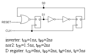
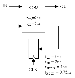
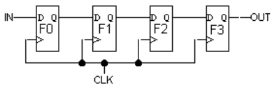 Each of the edge-triggered D flip-flops has a setup time of tS, a
hold time of tH, a propagation delay of tPD and a contamination delay
of tCD. Assume that IN is stable tS before the rising edge of CLK and
tH after the rising edge of CLK.
Each of the edge-triggered D flip-flops has a setup time of tS, a
hold time of tH, a propagation delay of tPD and a contamination delay
of tCD. Assume that IN is stable tS before the rising edge of CLK and
tH after the rising edge of CLK.
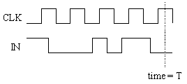 What is the value of OUT at time T?
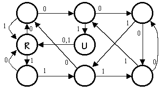
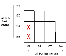
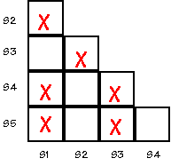
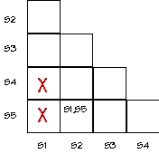
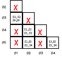
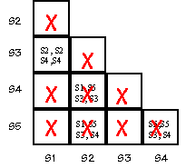
 Let's see if there is an equivalent state machine with fewer states
by checking to see if any states in the diagram above are equivalent.
Two states are equivalent if (1) they have identical outputs and (2)
for each possible combination of inputs they transition to equivalent
states.
Let's see if there is an equivalent state machine with fewer states
by checking to see if any states in the diagram above are equivalent.
Two states are equivalent if (1) they have identical outputs and (2)
for each possible combination of inputs they transition to equivalent
states.
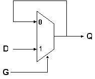 Recall that the MUX selects the Q output when G=0, and the D input
when G=1. The plan is that when G=1, the Q output will follow D after
a short delay; when G=0, the current Q output will be "latched" via
the feedback path. In this problem we explore assumptions necessary
to construct an informal proof that the latch behaves as proposed.
Assume, in each of the following, that the MUX is a well-behaved
lenient combinational device with a propagation delay of tpd.
Recall that the lenience of the MUX allows us to assume that if any
two of its inputs sufficient to determine its output are stable and
valid for at least tpd, then the MUX output will be stable and valid.
Recall that the MUX selects the Q output when G=0, and the D input
when G=1. The plan is that when G=1, the Q output will follow D after
a short delay; when G=0, the current Q output will be "latched" via
the feedback path. In this problem we explore assumptions necessary
to construct an informal proof that the latch behaves as proposed.
Assume, in each of the following, that the MUX is a well-behaved
lenient combinational device with a propagation delay of tpd.
Recall that the lenience of the MUX allows us to assume that if any
two of its inputs sufficient to determine its output are stable and
valid for at least tpd, then the MUX output will be stable and valid.