Problem 1. A 3:1 multiplexer has the following inputs and output:
-
three data inputs D0, D1 and D2
two select inputs S0 and S1
one data output Y
-
Y = D0 if S0 = 0 and S1 = 0
Y = D1 if S0 = 1 and S1 = 0
Y = D2 if S1 = 1 (the value S0 doesn't matter)
-
Write a Verilog module for the 3:1 multiplexer that implements the
sum-of-products equation for Y:
    __ __         __
Y = S0*S1*D0 + S0*S1*D1 + S1*D2
Use a dataflow style for your code (ie, use "assign" to set the values of your signals).module mux31_1(d0,d1,d2,s0,s1,y); input d0,d1,d2,s0,s1; output y; assign y = (~s0 & ~s1 & d0) | (s0 & ~s1 & d1) | (s1 & d2); endmodule
-
Write a Verilog module for the 3:1 multiplexer that uses the "?"
operator. Again use a dataflow style for your code (ie, use "assign"
to set the values of your signals).
module mux31_2(d0,d1,d2,s0,s1,y);
  input d0,d1,d2,s0,s1;
  output y;

  assign y = s1 ? d2 : (s0 ? d1 : d0);
endmodule
-
Write a Verilog module for the 3:1 multiplexer that uses the "case"
statement. Remember that a "case" statement can only appear inside
of a behavioral block.
module mux31_3(d0,d1,d2,s0,s1,y);
  input d0,d1,d2,s0,s1;
  output y;

  // add reg declarations for variables assigned inside of
  // the behavioral block below
  reg y;

  always @ (d0 or d1 or d2 or s0 or s1)
  begin
    case ({s1,s0})
     2'b00: y <= d0;
     2'b01: y <= d1;
     2'b10, 2'b11: y <= d2;
    endcase
  end
endmodule
Problem 2. When creating a behavioral block using Verilog's ALWAYS statement, one supplies a sensitivity list -- a list of signals that trigger execution of the block when they change value. For example, here's full adder module which uses an ALWAYS block:module fulladder(a,b,cin,sum,cout); input a,b,cin; output sum,cout; reg sum,cout; always @ (a or b or cin) begin sum <= a ^ b ^ cin; cout <= (a & b) | (a & cin) | (b & cin); end endmoduleWhen writing behavioral implementations of combinational logic all the signals appearing on the right-hand side of assignment statements (ie, signals whose values are used in computations) should appear in the sensitivity list.-
What would be the effect of, say, omitting cin from the sensitivity
list above?
Omitting cin from the sensitivity list would mean that during simulation changes in cin wouldn't trigger execution of the ALWAYS block, so the values of sum and cout wouldn't be recomputed to reflect the new value of cin.
The omission of a variable from the sensitivity list doesn't usually affect what logic is synthesized for the ALWAYS block. Of course, the logic gates will propagate changes in cin to sum and cout.
What's troublesome is that the simulation results are different from the results produced by the actual logic. This isn't so bad when the simulation results are discovered to be wrong and the source code gets fixed. It's much worse when the simulation gives the desired answer, but the synthesized logic (which may have already been delivered to a customer) does the wrong thing, ie, the incorrect simulation masked a bug in logic equations. Nowadays, many synthesizers give warnings when synthesizing combinational logic using values not declared in the sensitivity list of an ALWYS block.
Problem 3. Using the Verilog parameter mechanism it's possible to write modules whose operation depends on parameters specified when the module is instantiated.-
Write a parameterized parity module that takes as input a vector
whose size is set by the parameter. The module has a single output
which is 1 if the number of 1's in the input vector is odd and 0
otherwise.
module parity(in,p);
  parameter N = 8;   // width of vector IN, default value is arbitrary
  input [N-1:0] in;
  output p;

  assign p = ^in;    // using XOR as a reduction operator
endmodule
-
How would one instantiate an instance of your module to compute
parity on the 16-bit wide data bus DATA[15:0]?
parity #(16) xxx(DATA[15:0],p); // xxx is the name of this instance
Some Verilog synthesizers (eg, MAX+plus II, the one we use) don't allow the syntax used above for setting module parameters. One can also write
parity xxx(DATA[15:0],p);
defparam xxx.N=16;  // in MAX+plus II, this has to follow the instantiation of xxx
Problem 4. Consider the following combinational circuit that adds to 8-bit numbers. The circuit includes carry-in (CIN) and carry-out (COUT) signals so that it can be cascaded to form wider adders.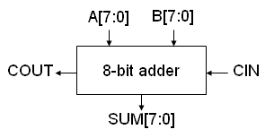
-
Where possible, it's best to use the built-in Verilog operators for
integer arithmetic. This makes it easy for the CAD tools to map your
logic onto the special-purpose arithmetic circuitry provided by many
of today's FPGAs. Write a Verilog module for the 8-bit adder that
uses the Verilog "+" operator. Use a dataflow style for your code
(ie, use "assign" to set the values of your signals).
module adder8_1(a,b,cin,sum,cout); input [7:0] a,b; input cin; output [7:0] sum; output cout; // Verilog knows that adding two N-bit numbers produces a (N+1)-bit // result. By concatenating cout and sum to form a 9-bit destination // for the add, we'll capture that high-order result bit. assign {cout,sum} = a + b + cin; endmodule-
A common method for building fast adders is to rewrite the equations
for SUM and COUT in terms of P (propagate) and G (generate) signals.
P is true if a carry-in will be propagated to the carry-out; G is
true if a carry-out will be generated regardless of the value of the
carry-in.
P = A ^ B     (^ is the xor operator)
G = A*B
SUM = P ^ CIN
COUT = G + P*CIN
The advantage of this formulation is that P and G can be computed in parallel for all the bits of the adder since they don't depend on CIN. This will shorten the delay between CIN and COUT. Write a Verilog module for the 8-bit adder that uses the P and G to compute SUM and COUT. Again use a dataflow style for your code.module adder8_2(a,b,cin,sum,cout); input [7:0] a,b; input cin; output [7:0] sum; output cout; wire [7:0] p,g,c; // P, G and COUT for each bit // all the lines below involve 8-bit wide operations assign p = a ^ b; assign g = a & b; assign c = g | (p & {c[6:0],cin}); // ripple carry! assign sum = p ^ {c[6:0],cin}; assign cout = c[7]; endmodule-
It can be hard to see how the carry chain is working in the
previous example. Sometimes it's easier to express what you
want if you use a loop and compute the answer bit-by-bit. Write
a Verilog module for the 8-bit adder that uses P and G, but this
time use a for-loop inside a behavioral block to compute SUM and
COUT bit-by-bit.
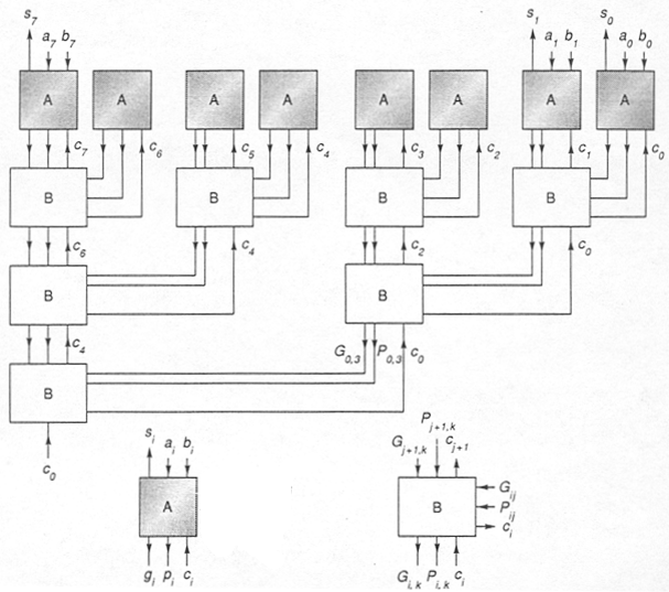
module adder8_3(a,b,cin,sum,cout);
  input [7:0] a,b;
  input cin;
  output [7:0] sum;
  output cout;

  // provide reg declarations for signals we'll be assigning
  // inside of the ALWAYS block below
  reg [7:0] sum;
  reg cout;
  reg c,p,g;
  integer i;    // index for for loop

  always @ (a or b or cin)     // we're sensitive to input changes
  begin
    c = cin;                   // carry-in to first stage
    // even though we appear to be reusing the c, p and g signals
    // each time through the loop, the synthesizer will realize it
    // needs to make local copies for each loop iteration.
    for (i = 0; i < 8; i = i + 1)
      begin
        p = a[i] ^ b[i];
        g = a[i] & b[i];
        sum[i] = p ^ c;
        c = g | (p & c);       // carry-in for next stage
      end
    cout = c;                  // final carry out
  end
endmodule
In the adder implementations above the carry ripples up through the bits starting with the least significant bit. The total propagation delay (tPD) of the circuit is determined by the logic along the path between CIN and COUT (known as the carry chain). In a ripple carry adder tPD is proportional to the number of bits in the adder.We can improve tPD by reworking the carry logic to use a "lookahead" strategy -- we'll use the P and G signals for individual nodes to compute P and G signals for pairs of nodes. We can apply this strategy again, computing P and G for groups of 4 nodes, and so on. We're building a tree of these lookahead modules; each node in the tree has the same logic. Once CIN for the adder is available it is fed to the top node of the lookahead tree, where it's combined with P and G of the children to produce carry-ins for the children nodes. This process continues until carry-in arrives at the leaf nodes where it can be used to compute SUM. For an N-bit adder, the depth of the lookahead tree is log2(N). It takes two traversals of the lookahead tree to (Ps and Gs up the tree, CINs down the tree) in order to finish the computation of SUM -- a tPD that's proportional to log2(N).
The following figure (from Hennessy and Patterson) shows what we have in mind.
-
Here are the logic equations for the outputs of the A module in the figure
above:
P = A ^ B
G = A * B
SUM = P ^ CIN
Write a Verilog implementation of the A module.module A(a,b,cin,p,g,sum); input a,b,cin; output p,g,sum; assign p = a ^ b; assign g = a & b; assign sum = p ^ cin; endmodule
-
Here are the logic equations for the outputs of the B module in the figure
above. P1 and G1 are the P and G signals from the right-hand connections
to the B block; P2 and G2 from the top connections.
POUT = P1*P2
GOUT = G2 + P2*G1
C1 = CIN
C2 = G1 + P1*CIN
Write a Verilog implementation of the B module.module B(p1,g1,p2,g2,cin,pout,gout,c1,c2); input p1,g1,p2,g2,cin; output pout,gout,c1,c2; // just for variety try a behavioral description reg pout,gout,c1,c2; always @ (p1 or g1 or p2 or g2 or cin) begin pout <= p1 & p2; gout <= g2 | (p2 & g1); c1 <= cin; c2 <= g1 | (p1 & cin); end endmodule-
Using the A and B modules you created above, write a Verilog module
for an 8-bit adder.
module adder8_4(a,b,cin,sum,cout);
  input [7:0] a,b;
  input cin;
  output [7:0] sum;
  output cout;

  // 8 A modules
  wire [7:0] p,g,c;
  A a0(a[0],b[0],c[0],p[0],g[0],sum[0]);
  A a1(a[1],b[1],c[1],p[1],g[1],sum[1]);
  A a2(a[2],b[2],c[2],p[2],g[2],sum[2]);
  A a3(a[3],b[3],c[3],p[3],g[3],sum[3]);
  A a4(a[4],b[4],c[4],p[4],g[4],sum[4]);
  A a5(a[5],b[5],c[5],p[5],g[5],sum[5]);
  A a6(a[6],b[6],c[6],p[6],g[6],sum[6]);
  A a7(a[7],b[7],c[7],p[7],g[7],sum[7]);

  // first layer of B modules
  wire [3:0] pp,gg,cc;
  B b_0(p[0],g[0],p[1],g[1],cc[0],pp[0],gg[0],c[0],c[1]);
  B b_1(p[2],g[2],p[3],g[3],cc[1],pp[1],gg[1],c[2],c[3]);
  B b_2(p[4],g[4],p[5],g[5],cc[2],pp[2],gg[2],c[4],c[5]);
  B b_3(p[6],g[6],p[7],g[7],cc[3],pp[3],gg[3],c[6],c[7]);

  // second layer of B modules
  wire [1:0] ppp,ggg,ccc;
  B bb_0(pp[0],gg[0],pp[1],gg[1],ccc[0],ppp[0],ggg[0],cc[0],cc[1]);
  B bb_1(pp[2],gg[2],pp[3],gg[3],ccc[1],ppp[1],ggg[1],cc[2],cc[3]);

  // final layer of B modules
  wire pppp,gggg;
  B bbb(ppp[0],ggg[0],ppp[1],ggg[1],cin,pppp,gggg,ccc[0],ccc[1]);

  // compute final carry out
  assign cout = gggg + (pppp & cin);
endmodule
-
Using the A and B modules you created above, write a Verilog module
for an 8-bit adder.
-
Here are the logic equations for the outputs of the B module in the figure
above. P1 and G1 are the P and G signals from the right-hand connections
to the B block; P2 and G2 from the top connections.
-
Here are the logic equations for the outputs of the A module in the figure
above:
-
It can be hard to see how the carry chain is working in the
previous example. Sometimes it's easier to express what you
want if you use a loop and compute the answer bit-by-bit. Write
a Verilog module for the 8-bit adder that uses P and G, but this
time use a for-loop inside a behavioral block to compute SUM and
COUT bit-by-bit.
-
A common method for building fast adders is to rewrite the equations
for SUM and COUT in terms of P (propagate) and G (generate) signals.
P is true if a carry-in will be propagated to the carry-out; G is
true if a carry-out will be generated regardless of the value of the
carry-in.
-
Where possible, it's best to use the built-in Verilog operators for
integer arithmetic. This makes it easy for the CAD tools to map your
logic onto the special-purpose arithmetic circuitry provided by many
of today's FPGAs. Write a Verilog module for the 8-bit adder that
uses the Verilog "+" operator. Use a dataflow style for your code
(ie, use "assign" to set the values of your signals).
-
How would one instantiate an instance of your module to compute
parity on the 16-bit wide data bus DATA[15:0]?
-
Write a parameterized parity module that takes as input a vector
whose size is set by the parameter. The module has a single output
which is 1 if the number of 1's in the input vector is odd and 0
otherwise.
-
What would be the effect of, say, omitting cin from the sensitivity
list above?
-
Write a Verilog module for the 3:1 multiplexer that uses the "case"
statement. Remember that a "case" statement can only appear inside
of a behavioral block.
-
Write a Verilog module for the 3:1 multiplexer that uses the "?"
operator. Again use a dataflow style for your code (ie, use "assign"
to set the values of your signals).