Problem 4. Consider the following combinational circuit that adds to 8-bit numbers. The circuit includes carry-in (CIN) and carry-out (COUT) signals so that it can be cascaded to form wider adders.
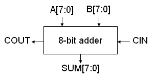
- Where possible, it's best to use the built-in Verilog operators for integer arithmetic. This makes it easy for the CAD tools to map your logic onto the special-purpose arithmetic circuitry provided by many of today's FPGAs. Write a Verilog module for the 8-bit adder that uses the Verilog "+" operator. Use a dataflow style for your code (ie, use "assign" to set the values of your signals).
-
A common method for building fast adders is to rewrite the equations
for SUM and COUT in terms of P (propagate) and G (generate) signals.
P is true if a carry-in will be propagated to the carry-out; G is
true if a carry-out will be generated regardless of the value of the
carry-in.
P = A ^ B     (^ is the xor operator)
G = A*B
SUM = P ^ CIN
COUT = G + P*CIN
The advantage of this formulation is that P and G can be computed in parallel for all the bits of the adder since they don't depend on CIN. This will shorten the delay between CIN and COUT. Write a Verilog module for the 8-bit adder that uses the P and G to compute SUM and COUT. Again use a dataflow style for your code.
- It can be hard to see how the carry chain is working in the previous example. Sometimes it's easier to express what you want if you use a loop and compute the answer bit-by-bit. Write a Verilog module for the 8-bit adder that uses P and G, but this time use a for-loop inside a behavioral block to compute SUM and COUT bit-by-bit.
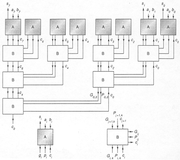
We can improve tPD by reworking the carry logic to use a "lookahead" strategy -- we'll use the P and G signals for individual nodes to compute P and G signals for pairs of nodes. We can apply this strategy again, computing P and G for groups of 4 nodes, and so on. We're building a tree of these lookahead modules; each node in the tree has the same logic. Once CIN for the adder is available it is fed to the top node of the lookahead tree, where it's combined with P and G of the children to produce carry-ins for the children nodes. This process continues until carry-in arrives at the leaf nodes where it can be used to compute SUM. For an N-bit adder, the depth of the lookahead tree is log2(N). It takes two traversals of the lookahead tree to (Ps and Gs up the tree, CINs down the tree) in order to finish the computation of SUM -- a tPD that's proportional to log2(N).
The following figure (from Hennessy and Patterson) shows what we have in mind.
-
Here are the logic equations for the outputs of the A module in the figure
above:
P = A ^ B
G = A * B
SUM = P ^ CIN
Write a Verilog implementation of the A module.
-
Here are the logic equations for the outputs of the B module in the figure
above. P1 and G1 are the P and G signals from the right-hand connections
to the B block; P2 and G2 from the top connections.
POUT = P1*P2
GOUT = G2 + P2*G1
C1 = CIN
C2 = G1 + P1*CIN
Write a Verilog implementation of the B module.
- Using the A and B modules you created above, write a Verilog module for an 8-bit adder.