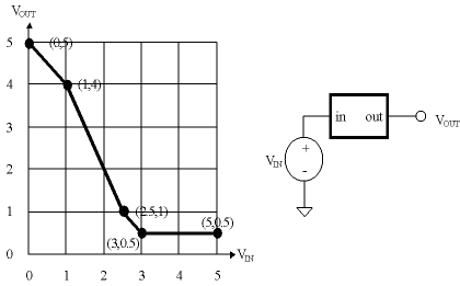
Problem 1. The behavior of a 1-input, 1-output device is measured by hooking a voltage source to its input and measuring the voltage at the output for several different input voltages:
-
if VIN <= VIL then VOUT >= VOH, and
if VIN >= VIH then VOUT <= VOL.
-
Can one chose a VOL of 0V for this device? Explain.
No, since the static discipline requires that VOUT <= VOL for a valid "0" output and VOUT for this device never falls below 0.5V.
-
What's the smallest VOL one can choose and still have the device obey
the static discipline? Explain.
The smallest VOL one can choose is 0.5V, the lowest output voltage produced by the device.
-
Assuming that we want to have 0.5V noise margins for both "0" and "1"
values, what are appropriate voltage levels for VOL,
VIL, VIH, and VOH so that the device
obeys the static discipline. Hint: there are many possible choices,
just choose one that obeys the constraints listed above.
Here are the rules of operation imposed on us by the static discipline:
- VIN >= VIH implies VOUT <= VOL
- VIN <= VIL implies VOUT >= VOH
- VOL + noise margin = VIL
- VOH - noise margin = VIH
-
applying rule 3: VIL = 1V
applying rule 2 and looking at the VTC: VOH = 4V
applying rule 4: VIH = 3.5V-
Assuming that we want to have 0.5V noise margins for both "0" and "1"
values, what is the largest possible voltage level for VOL that still
results in a device that obeys the static discipline?
To determine our maximum VOL, let's set it equal to N. Then
-
VIL = N + 0.5V
-
VIH = VIL + M = N + 0.5 + M.
-
VOH = VIH + 0.5 = N + M + 1.
-
VOH = VTC(VIL) implies N + M + 1 = VTC(N + 0.5) = 6 - 2*(N + 0.5)
VOL = VTC(VIH) implies N = VTC(N + 0.5 + M) = 6 - 2*(N + M + 0.5)-
Assuming that we want to have equal noise margins for both "0" and "1"
values, what is the largest noise margin we can achieve with this
device and still obey the static discipline?
It's clear that to maximize our noise margins, VOL should be as small as possible and VOH should be as large as possible. By inspecting the VTC we see that VOL = 0.5V is the best we can do. From earlier parts we know we can achieve a noise margin N of at least 0.5V. We can use the following construction to figure out the largest noise margin N. Consider two of these devices hooked in series:
-
at point "B", the largest voltage we'll measure is 0.5 + N, i.e.,
the voltage we applied to the other end of the wire and the worst-case
noise perturbation.
referring to the VTC, with 0.5+N on the input we'll measure a voltage
of 4 - 2(N + .5 - 1) = 5 - 2N at the output (point "C").
at point "D", the smallest voltage we'll measure is 5 - 3N, i.e.,
the voltage we applied to the other end of the wire and the worst-case
noise perturbation.
finally at point "E" we'd want to measure 0.5V, i.e., a valid "0"
voltage level.
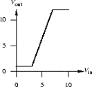
Problem 2. Inverter madness.-
The following graph plots the voltage transfer characteristic
for a device with one input and one output.
 No. The device doesn't have any region in which its gain is greater than 1, so there are no choices for VIL, VOL, VIH, VOH which provide for non-zero noise margins.
-
You are designing a new logic family and trying to decide on values
of the four parameters VIL, VOL, VIH,
VOH that lead to non-zero noise margins for various
possible inverter designs. Four proposed inverter designs exhibit the
voltage transfer characteristics shown in the diagrams below. For
each design, either (1) specify suitable values of VIL,
VOL, VIH, VOH. or (2) explain why no
values for these parameters satisfy the static discipline.
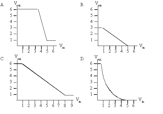 Device A: VOL = 1V, VIL = 3.5V, VIH = 5V, VOH = 6V Device B: no values exist, the gain is never greater than one Device C: no values exist, the gain is never greater than one Device D: VOL = .5V, VIL = 1V, VIH = 3.5V, VOH = 6V
Problem 3. Static discipline.-
Consider a combinational buffer with one input and one output.
Suppose we set its input to some voltage (VIN), wait for
the device to reach a steady state, then measure the voltage on its
output (VOUT) and find VOUT < VOL.
What can we say about VIN?
A combinational device guarantees that valid inputs lead to valid outputs if we wait longer than the propagation delay. But the opposite inference isn't true: a valid output doesn't imply a valid input -- for example, the buffer is allowed a valid "1" before the input has crossed VIH. So the only statement that we can make is that VIN < VIH since if VIN >= VIH the buffer is required to produce VOUT >= VOH.
-
Now consider an inverter. Suppose we set its inputs to some voltage
(VIN), wait for the device to reach a steady state, then
measure the voltage on its output (VOUT) and find
VOUT > VOH. What can we say about
VIN?
Using the same argument as above, the only statement we can make is that VIN < VIH.
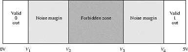
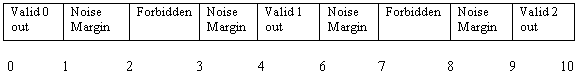
Problem 4. Ternary Logic. Ternary is a term referring to the number system in base 3. Consider a convention in which a ternary digit is presented as an electric voltage between 0 and 10 V. Let 0-1 V represent a valid "0" output, 4-6 V a valid "1" output and 9-10 V a valid "2" output.-
Assuming noise margins 1 V wide, show the mapping of logic levels to
voltages for this ternary system. Include valid logic-level outputs,
noise margins and forbidden zones. Your chart should resemble the
following diagram, except of course it will incorporate 3 valid signal
levels:
-
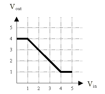
Graph the transfer characteristic for a device capable of acting as a
ternary logic buffer, i.e., a device that produces at its output the
same logic level present at its input, as shown below:
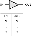 We need three "stable" regions, one for each valid output, and a high gain between valid levels to help restore poor inputs to an output valid level.
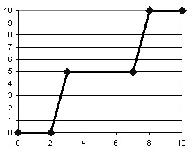
-
Can a device with the following transfer characteristic be used as
a ternary logic buffer? Why or why not?
 No, it can't be used as a ternary logic buffer. The device has only two "stable" regions.
Problem 5. Bread and Circuits, Inc. has discovered an interesting electronic device (a Z-module) which is made using a single yeast cell, a speck of flour, and a grain of salt. The Z-module has two inputs carrying voltages VA and VB and a single output carrying VC. The output VC settles, after a 10ns period of stable input voltages, to the product of the input voltages restricted to range of 0V to 2V. In other words,
Assume that the Z-module treats negative input voltages as if they were 0. B&C is trying to make a logic family using Z-modules. As a starting point, they claim thatVC = VA * VB when 0 <= VA * VB <= 2 2 when VA * VB > 2 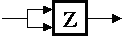
-
Which, if any, of the following proposed voltage thresholds yields a
valid buffer with positive noise margins?
A. VOL = 1.5V  VIL = 1.6V  VIH = 1.7V  VOH = 1.8V
B. VOL = 0.7V  VIL = 0.9V  VIH = 1.1V  VOH = 1.3V
C. VOL = 0.1V  VIL = 0.3V  VIH = 1.7V  VOH = 1.9V
D. VOL = 0.5V  VIL = 0.5V  VIH = 1.5V  VOH = 1.5V
Choice A would allow two "low" inputs (e.g., 1.6V) to generate a "high" output (1.6 * 1.6 = 2.56 which is above VOH) => not okay. Choice B would allow two "high" inputs (e.g., 1.1V) to generate an underdetermined output (1.1 * 1.1 = 1.21 which is above VOL but below VOH) => not okay. Choice C has positive noise margins and the allowed input voltages result in the desired behavior => okay Choice D doesn't have positive noise margins => not okay.-
Determine the voltage thresholds that maximize the noise margins of
B&C's buffer. If the noise margins are not independent, maximize the
smaller of the two.
To maximize the noise margins of the buffer, we consider the voltage transfer characteristic of the Z-module. Since VIN2 >= 2 will result in a VOH of 2, then we have VIH >= sqrt(2). Thus, VIH = sqrt(2), and VOH = 2. Since VOUT = VIN2 in the lower region of the voltage transfer characteristic, then let us represent VIN with "x" and VOUT with "x2". Then the lower noise margin is represented by the function f(x) = x - x2. To maximize the noise margin, we take the first derivative of f(x) and set it to zero: f'(x) = 1 - 2x = 0. Solving for x gives 0.5. Thus, VIL = x = 0.5V, and VOL = x2 = 0.25V.
-
Ivan Idea, chief logician at B&C, is exploring the use of a single
Z-module as a two-input logic gate, again with positive noise margins.
He suspects that a Z-module, under the appropriate logic conventions,
can be used for an AND or OR gate which obeys the static discipline.
Ivan's been at it for several weeks and needs your help.
Can you find a way to use a Z-module for an AND or OR combinational
device? If so, give the appropriate input and output voltage
thresholds and the function performed. If not, carefully explain why
the Z-module can't be used as AND or OR.
No, the Z-module can't be used as either an AND gate or an OR gate. In order to implement an OR gate, we must have the behavior that a logic "1" input and a logic "0" input produces a logic "1" output. In the case of a single Z-module, if we had 2V as the first input and 0V as the second input (noiseless, perfect input voltages) the output is 0V, instead of a logic "1" voltage. In order to implement an AND gate, we must have the behavior that a logic "1" input and a logic "0" input produces a logic "0" output. According to the static discipline, a "0" output means VOUT should be less than equal to VOL. If we substitute 2V for the logic "1" input and consider the "0" input, we have VOUT = VIL * 2 <= VOL. But we can't have VOL > VIL, so the Z-module can't function as an AND gate.
-
Ivan sidesteps the previous enigma by allowing himself the use of
several Z-modules as components of a single logic gate. He assumes
(and you may too) that noise enters the system only between logic
gates, not between the components of a single gate. He notes that
each of B&C's proposed buffers (using one Z-module) is an amplifier
with gain greater than one. Ivan reasons that by cascading many such
devices (as shown below), he can achieve arbitrarily high gain and
hence excellent noise margins.
 For N cascaded Z-modules, the voltage transfer characteristic is:
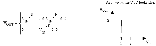
-
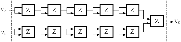
Is there any way by which many Z-modules can be used to build a
2-input AND gate whose noise margins are both greater than 0.75V? If
so, sketch an approach (giving a diagram and calculating the noise
margins). If not, give a brief but convincing explanation.
It is possible to build an AND gate whose noise margins greater than 0.75V. Our strategy is to clean up both input signals independently before computing the logic function. A cascade of 5 Z-modules is enough to restore marginal signals, and the last Z-module on the right performs the AND function. The diagram looks like this:
Problem 6. Combinational construction rules In lecture, we learned two basic principles regarding the class of combinational devices. The first allows us to build a combinational device from, e.g., electronic components:- A combinational device is a circuit element that has
- one or more digital inputs
- one or more digital outputs
- a functional specification that details the value of each output for every possible combination of valid input values
- a timing specification consisting (at minimum) of an upper bound tpd on the required time for the device to compute the specified output values from an arbitrary set of stable, valid input values.
- A set of interconnected elements is a combinational device if
- each circuit element is combinational
- every input is connected to exactly one output or to some vast supply of 0's and 1's
- the circuit contains no directed cycles
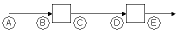
-
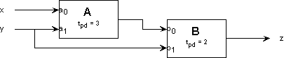
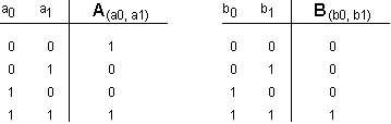
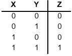
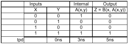
Give a truth table for the acyclic circuit, i.e. a table that
specifies the value of z for each of the possible combinations of
input values on x and y.
-
Describe a general procedure by which a truth table can be computed
for each output of an arbitrary acyclic circuit containing only
combinational components. [HINT: construct a functional specification to
each circuit node].
Since each circuit node is connected to an output of some combinational element, the functional specification for each circuit node is given by the functional specification for the combinational element which drives it. If we start with components that are only connected to inputs to the overall circuit, we can build truth tables for their outputs that only involve those inputs. We can then work on the next tier of components and build truth tables for their outputs that only involve overall circuit inputs. Continuing in this manner, we'll eventually reach components that drive the overall circuit outputs and be able to construct truth tables for each output that only involves overall circuit inputs. In our example, we'd first build a truth table for the output of the A module and then use that table to build a table for Z:
-
Specify a propagation delay (the upper bound required for each
combinational device) for the circuit.
The propagation delay for Z is 5ns.
-
Describe a general procedure by which a propagation delay can be
computed for an arbitrary acyclic circuit containing only
combinational components. [HINT: add a timing specification to each
circuit node].
- Label each INPUT to the circuit with tpd=0.
- Repeatedly
- Find a circuit element E whose input nodes are each labeled with a prop delay but whose output nodes are not.
- Label each output node of E with the delay M, where M is the prop delay of E plus the MAXIMUM of the times on the input nodes.
- When you can't find an unlabeled output node, stop.
- The prop delay spec for the device is the MAX of the prop delay labels on the output nodes.
-
Do your general procedures for computing functional specifications and
propagation delays work if the restriction to acyclic circuits is
relaxed? Explain.
No. Without cycles, you're guaranteed to be able to find a new output node to label (i.e., the output of some element E whose inputs are already labeled) until the entire circuit is labeled. If you have cycles, the algorithm breaks down. You can be left with a cycle of elements whose outputs are unlabeled and some of whose inputs are unlabeled.
Problem 7. If you are given the following 2-input and 2-output combinational block: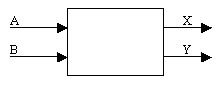
-
Does this device adhere to the static disipline?
Yes: there's an unambiguous functional specification for each output and a maximum propagation delay has been specified.
-
Suppose that the output X is connected to the input B, what
output would you expect?
If you assume that the circuit was composed of two inverters (one with A as its input, the other with B as its input) then we would expect Y = A after 2 second propagation delay. However, there are other implementations that have the same functional specification. In particular, X might be implemented with logic that uses both A and B as inputs. In this case, connecting X to B would create a cycle and the value of Y might be undetermined.
-
Suppose the functional description was changed to the
following: The ouput X is a 1 if both A and B are "0", and
Y is a 1 if either A or B but not both are "1".
Does this change the answer the previous question?
No. Since X and Y are functions of both A and B, it's more obvious that a cycle would be created when X was connected to B.
-
Suppose the functional description was changed to the
following: The ouput X is a 1 if both A and B are "0", and
Y is a 1 if either A or B but not both are "1".
Does this change the answer the previous question?
-
Suppose that the output X is connected to the input B, what
output would you expect?
-
Does this device adhere to the static disipline?
-
Describe a general procedure by which a propagation delay can be
computed for an arbitrary acyclic circuit containing only
combinational components. [HINT: add a timing specification to each
circuit node].
-
Specify a propagation delay (the upper bound required for each
combinational device) for the circuit.
-
Describe a general procedure by which a truth table can be computed
for each output of an arbitrary acyclic circuit containing only
combinational components. [HINT: construct a functional specification to
each circuit node].
- A combinational device is a circuit element that has
-
Is there any way by which many Z-modules can be used to build a
2-input AND gate whose noise margins are both greater than 0.75V? If
so, sketch an approach (giving a diagram and calculating the noise
margins). If not, give a brief but convincing explanation.
-
Ivan sidesteps the previous enigma by allowing himself the use of
several Z-modules as components of a single logic gate. He assumes
(and you may too) that noise enters the system only between logic
gates, not between the components of a single gate. He notes that
each of B&C's proposed buffers (using one Z-module) is an amplifier
with gain greater than one. Ivan reasons that by cascading many such
devices (as shown below), he can achieve arbitrarily high gain and
hence excellent noise margins.
-
Ivan Idea, chief logician at B&C, is exploring the use of a single
Z-module as a two-input logic gate, again with positive noise margins.
He suspects that a Z-module, under the appropriate logic conventions,
can be used for an AND or OR gate which obeys the static discipline.
Ivan's been at it for several weeks and needs your help.
Can you find a way to use a Z-module for an AND or OR combinational
device? If so, give the appropriate input and output voltage
thresholds and the function performed. If not, carefully explain why
the Z-module can't be used as AND or OR.
-
Determine the voltage thresholds that maximize the noise margins of
B&C's buffer. If the noise margins are not independent, maximize the
smaller of the two.
-
Which, if any, of the following proposed voltage thresholds yields a
valid buffer with positive noise margins?
-
Can a device with the following transfer characteristic be used as
a ternary logic buffer? Why or why not?
-
Graph the transfer characteristic for a device capable of acting as a
ternary logic buffer, i.e., a device that produces at its output the
same logic level present at its input, as shown below:
-
Assuming noise margins 1 V wide, show the mapping of logic levels to
voltages for this ternary system. Include valid logic-level outputs,
noise margins and forbidden zones. Your chart should resemble the
following diagram, except of course it will incorporate 3 valid signal
levels:
-
Now consider an inverter. Suppose we set its inputs to some voltage
(VIN), wait for the device to reach a steady state, then
measure the voltage on its output (VOUT) and find
VOUT > VOH. What can we say about
VIN?
-
Consider a combinational buffer with one input and one output.
Suppose we set its input to some voltage (VIN), wait for
the device to reach a steady state, then measure the voltage on its
output (VOUT) and find VOUT < VOL.
What can we say about VIN?
-
You are designing a new logic family and trying to decide on values
of the four parameters VIL, VOL, VIH,
VOH that lead to non-zero noise margins for various
possible inverter designs. Four proposed inverter designs exhibit the
voltage transfer characteristics shown in the diagrams below. For
each design, either (1) specify suitable values of VIL,
VOL, VIH, VOH. or (2) explain why no
values for these parameters satisfy the static discipline.
-
The following graph plots the voltage transfer characteristic
for a device with one input and one output.
-
Assuming that we want to have equal noise margins for both "0" and "1"
values, what is the largest noise margin we can achieve with this
device and still obey the static discipline?
-
Assuming that we want to have 0.5V noise margins for both "0" and "1"
values, what are appropriate voltage levels for VOL,
VIL, VIH, and VOH so that the device
obeys the static discipline. Hint: there are many possible choices,
just choose one that obeys the constraints listed above.
-
What's the smallest VOL one can choose and still have the device obey
the static discipline? Explain.