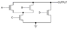
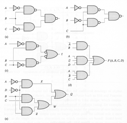
Problem 1. The following diagram shows a schematic for the pulldown circuitry for a particular CMOS gate:
-
What is the correct schematic for the pullup
circuitry?
To figure out the complement of a FET circuit, decompose it into SERIES and PARALLEL subcircuits. In our example the NFET pulldown circuitry can be decomposed as:
PARALLEL(SERIES(PARALLEL(A,B),C),D) The complementary circuit simply converts SERIES circuits into PARALLEL circuits and vice versa:SERIES(PARALLEL(SERIES(A,B),C),D) which we can then draw as a schematic using the complementary type of FET (in this example PFETs):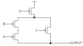
-
Assuming the pullup circuitry is designed correctly, what is
the logic function implemented this gate?
Start with the SERIES/PARALLEL decomposition of the pulldown given in the answer to the preceeding question:
PARALLEL(SERIES(PARALLEL(A,B),C),D) Convert SERIES connections to AND and PARALLEL connections to OR:OR(AND(OR(A,B),C),D) Finally invert the answer to getOUTPUT = -(D + C*(A + B)) where "-" is NOT, "*" is AND and "+" is OR.-
Assuming the pullup circuitry is designed
correctly, when the output of the CMOS gate above
is a logic "0", in the steady state what would we
expect the voltage of the output terminal to be?
What would be the voltage if the output were a
logic "1"?
When the output of a CMOS gate is a logic "0", we would expect the voltage to be essentially 0V. There is a miniscule amount of leakage through the pullup circuitry even though the PFETS are off, so the output isn't precisely 0V, but the current through the NFET pulldowns is many of order of magnitude larger. Similarly, when the output of a CMOS gate is a logic "1", we would expect the voltage to be the same as the power supply voltage (VDD).
Problem 2. The following diagram shows a schematic for the pullup circuitry for a particular CMOS gate:
-
Draw a schematic for the pulldown circuitry for this CMOS gate.
The pullup is configured as SERIES(PARALLEL(A,D),PARALLEL(B,C)) so the pulldown should be the complement: PARALLEL(SERIES(A,D),SERIES(B,C))

-
Assuming the pulldown circuitry is designed correctly, give an expression
for the logic function implemented by this gate.
Using the pullup circuitry we can develop the following sum-of-products expression for F:
     _   _   _   _    _ _   _ _   _ _   _ _
F = (A + D)*(B + C) = A*B + A*C + B*D + C*D
Or we can look at the pulldown circuitry and express F as the complement of the function that describes when the pulldown is on:_________ F = A*D + B*C
Using several applications of DeMorgan's theorem this can be expanded to___ ___ _ _ _ _ F = (A*D)*(B*C) = (A + D)*(B + C)
which is the expression we derived using the pullup circuitry.
Problem 3. Consider the following circuit built from nfets and pfets:
-
Can this circuit be used as a CMOS gate? If not,
explain why. If so, what function does it compute?
Since the pullup and pulldown circuits are complementary, the circuit is a legitimate CMOS gate. The function is
    _________    ___  _    _   _  _   _ _   _ _
F = (A*B) + C = (A*B)*C = (A + B)*C = A*C + B*C
Problem 4. Consider the 4-input Boolean function Y = (A*B) + (C*D) where "*" is AND and "+" is OR.-
Implement the function with a single 4-input CMOS gate and an inverter.
Problem 5. Anna Logue, a circuit designer who missed several early 6.111 lectures, is struggling to design her first CMOS logic gate. She has implemented the following circuit: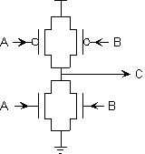
-
What is burning out Anna's test chips? Give a specific scenario,
including input values together with a description of the failure
scenario. For what input combinations will this failure occur?
The chips are burning out when the pulldown and pullup are both active. This will occur when A=0, B=1 or when A=1, B=0.
-
Are there input combinations for which Anna can expect a valid output at C? Explain.
Yes, if A=1 and B=1, then C=0. Or if A=0 and B=0, then C=1
-
One of Anna's test chips has failed by burning out the pullup
connected to A as well as the pulldown connected to B. Each of the
burned out FETs appears as an open circuit, but the rest of the
circuit remains functional. Can the resulting circuit be used as a
combinational device whose two inputs are A and B?
Explain its behavior for each combination of
valid inputs.
No. When A=1 and B=0, the circuit will burn out again, since the pullup and pulldown will be active, thus burning out the circuit. Also, the output is not defined when A=0 and B=1, since neither the pullup or pulldown are active.
-
In order to salvage her remaining three chips, Anna connects the A and
B inputs of each and tries to use it as a single-input gate. Can the
result be used as a single-input combinational device? Explain.
Yes. Since A=B, we are left with the following function (an inverter):
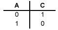
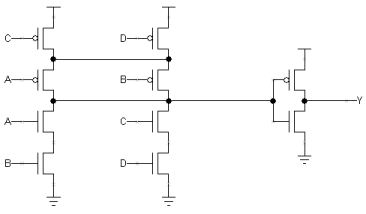
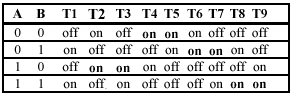
Problem 6. Occasionally you will come across a CMOS circuit where the complementary nature of the n-channel pull-downs and p-channel pull-ups are not obvious, as in the circuit shown below: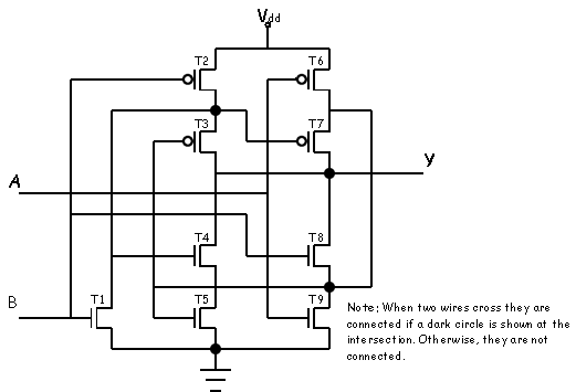
-
Construct a table that gives the on-off status of each transistor in
the circuit above for all combinations of inputs A and B.
-
Compute the output, Y, for each input combination and describe the
function of the above circuit.
The output Y is connected to four pairs of transistors in series, so each of these pairs can affect the output.
-
when A=0 and B=0, transistors T4 and T5 are on, so Y=0
when A=0 and B=1, transistors T6 and T7 are on, so Y=1
when A=1 and B=0, transistors T2 and T3 are on, so Y=1
when A=1 and B=1, transistors T8 and T9 are on, so Y=0
Problem 7. Consider the following circuit that implements the 2-input function H(A,B):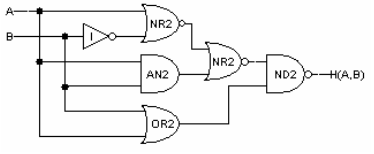
-
Fill in the following truth table for H:
A B H 0 0 0 1 1 0 1 1 A B H 0 0 1 0 1 1 1 0 0 1 1 1 -
Give a sum-of-products expression that corresponds to the truth table above.
The equation has one product term for each line of the truth table where H(A,B) = 1. Each product term contains two literals, one for each of the two inputs.
    _ _         _
H = A*B + A*B + A*B
-
Using the following table of timing specifications for each component,
what are tCD and tPD for the circuit
shown above?
gate tCD tPD I 3ps 15ps ND2 5ps 30ps AN2 12ps 50ps NR2 5ps 30ps OR2 12ps 50ps tCD = cd(NR2) + cd(NR2) + cd(ND2) = 15ps- = minimum considering all paths from inputs to output
- = maximum considering all paths from inputs to output
Problem 8. Gates and Boolean equations-
Show the Boolean equation for the function F described by the
following circuit:
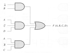
_ _ _ F(A,B,C,D) = A*B + A*C*D + A*B*C-
Consider the circuit shown below. Each of the control inputs, C0
through C3, must be tied to a constant, either 0 or 1.
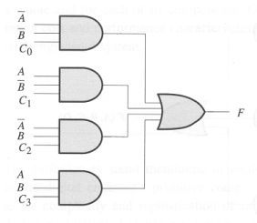 What are the values of C0 through C3
that would cause F to be the exclusive OR
of A and B?
We want F to be 1 when A=1 and B=0, or when A=0 and B=1. So C0 = 0, C1 = 1, C2 = 1, C3 = 0.
What are the values of C0 through C3
that would cause F to be the exclusive OR
of A and B?
We want F to be 1 when A=1 and B=0, or when A=0 and B=1. So C0 = 0, C1 = 1, C2 = 1, C3 = 0.-
Can any arbitrary
Boolean function of A and B be realized through appropriate wiring of the
control signals C0 through C3?
Yes. This circuit implements a 4-input MUX with its two select lines connected to A and B. By choosing the appropriate values for C0 through C3 we can implement any of the 16 possible Boolean functions of A and B.
-
Give a sum-of-products expression for each of the
following circuits:
_ _ (A) = A*B + B + C _ _ (B) = A*C + B*C _ _ (C) = A*C + B*C _ _ _ (D) = A*B + A*C*D + A*B*C _ _ _ (E) = A*D + B*C + B*D-
Give a canonical sum-of-products expression for the Boolean function
described by each truth table below
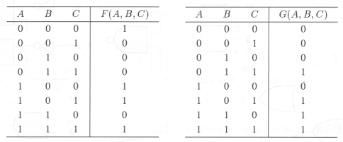 We can construct a sum-of-products expression from a truth table by writing down a product term for each line of the table where the output is 1. Each product term contains all the input variables: directly (ie, "A") if that variable is 1 for this line of the truth table, or negated (ie, "not A") if that variable is 0 for this line of the truth table. We then OR the product terms together to get the final expression:
_ _ _ _ _ _ F(A,B,C) = A*B*C + A*B*C + A*B*C + A*B*C _ _ _ G(A,B,C) = A*B*C + A*B*C + A*B*C + A*B*C-
We've seen that there are a total of sixteen 2-input Boolean
functions. How many 5-input Boolean functions are there?
There are 225 = 232 5-input boolean functions. To see why, recall that the truth table for a 5-input function will have 32 rows, one for each possible combination of the 5 inputs. The output column for each row can be filled in with one of two choices ("0" or "1"), for a total of 232 possible ways of filling in the output column for all 32 rows.
Problem 9. A priority encoder has inputs that are assigned some predetermined order. The output is the binary encoding of the first "1" valued input from the ordered list, and it is zero otherwise.-
Give the truth table for a 3-input priority encoder.
Assume the inputs are A, B, C with A having priority 3, B priority 2 and C priority 1:
A  B  C | P1 P0
========|=========
0  0  0 |  0  0
0  0  1 |  0  1
0  1  0 |  1  0
0  1  1 |  1  0
1  0  0 |  1  1
1  0  1 |  1  1
1  1  0 |  1  1
1  1  1 |  1  1
-
Give a sum of products realization of this priority encoder.
     _   _   _         _ _     _         _
P1 = A*B*C + A*B*C + A*B*C + A*B*C + A*B*C + A*B*C = A + B
     _ _       _ _     _         _               _
P0 = A*B*C + A*B*C + A*B*C + A*B*C + A*B*C = A + B*C
Problem 10. Suppose we are building circuits using only the following three components:- inverter: tcd = 0.5ns, tpd = 1.0ns, tr = tf = 0.7ns
- 2-input NAND: tcd = 0.5ns, tpd = 2.0ns, tr = tf = 1.2ns
- 2-input NOR: tcd = 0.5ns, tpd = 2.0ns, tr = tf = 1.2ns

-
What is tPD for this circuit?
tPD for the circuit is the maximum cumulative propagation delay considering all paths from any input to any output. In this circuit, the longest path involves three 2-input NAND gates with a cummulative tPD = 6ns.
-
What is tCD for this circuit?
tCD for the circuit is the minimum cumulative contamination delay considering all paths from any input to any output. In this circuit, the shortest path involves two 2-input NAND gates with a cumulative tCD = 1ns.
-
What is tPD of the fastest equivalent
circuit (i.e., one that implements the same function)
built using only the three components listed above?
The most straightforward way to determine the functionality of a circuit is to build a truth table:
A  B  | OUT
======|=====
0  0  |  1
0  1  |  0
1  0  |  1
1  1  |  0
from which we can see that OUT = not B. We can implement this with a single inverter that has a tPD = 1ns.
Problem 11. Suppose that each component in the circuit below has a propagation delay (tpd) of 10ns, a contamination delay (tcd) of 1ns, and negligable rise and fall times. Suppose initially that all four inputs are 1 for a long time and then the input D changes to 0.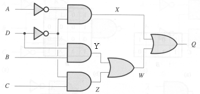
-
Draw a waveform plot showing how X, Y, Z, W and
Q change with time after the input transition on D.

-
Draw a waveform plot showing how X, Y, Z, W and
Q change with time after the input transition on D.
-
What is tPD of the fastest equivalent
circuit (i.e., one that implements the same function)
built using only the three components listed above?
-
What is tCD for this circuit?
-
Give a sum of products realization of this priority encoder.
-
Give the truth table for a 3-input priority encoder.
-
We've seen that there are a total of sixteen 2-input Boolean
functions. How many 5-input Boolean functions are there?
-
Give a canonical sum-of-products expression for the Boolean function
described by each truth table below
-
Give a sum-of-products expression for each of the
following circuits:
-
Can any arbitrary
Boolean function of A and B be realized through appropriate wiring of the
control signals C0 through C3?
-
Consider the circuit shown below. Each of the control inputs, C0
through C3, must be tied to a constant, either 0 or 1.
-
Show the Boolean equation for the function F described by the
following circuit:
-
Using the following table of timing specifications for each component,
what are tCD and tPD for the circuit
shown above?
-
Give a sum-of-products expression that corresponds to the truth table above.
-
Fill in the following truth table for H:
-
Compute the output, Y, for each input combination and describe the
function of the above circuit.
-
Construct a table that gives the on-off status of each transistor in
the circuit above for all combinations of inputs A and B.
-
In order to salvage her remaining three chips, Anna connects the A and
B inputs of each and tries to use it as a single-input gate. Can the
result be used as a single-input combinational device? Explain.
-
One of Anna's test chips has failed by burning out the pullup
connected to A as well as the pulldown connected to B. Each of the
burned out FETs appears as an open circuit, but the rest of the
circuit remains functional. Can the resulting circuit be used as a
combinational device whose two inputs are A and B?
Explain its behavior for each combination of
valid inputs.
-
Are there input combinations for which Anna can expect a valid output at C? Explain.
-
What is burning out Anna's test chips? Give a specific scenario,
including input values together with a description of the failure
scenario. For what input combinations will this failure occur?
-
Implement the function with a single 4-input CMOS gate and an inverter.
-
Can this circuit be used as a CMOS gate? If not,
explain why. If so, what function does it compute?
-
Assuming the pulldown circuitry is designed correctly, give an expression
for the logic function implemented by this gate.
-
Draw a schematic for the pulldown circuitry for this CMOS gate.
-
Assuming the pullup circuitry is designed
correctly, when the output of the CMOS gate above
is a logic "0", in the steady state what would we
expect the voltage of the output terminal to be?
What would be the voltage if the output were a
logic "1"?
-
Assuming the pullup circuitry is designed correctly, what is
the logic function implemented this gate?