Problem 1. The Motorola MCM6264 integrated circuit is a 8Kx8 static RAM. When answering the following questions about the timing of its various signals please refer to the data sheet. Assume you are using the -12 version of the MCM6264.
-
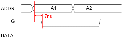
The timing diagram below shows two READ accesses, one for location A1 and the other
for location A2.
Complete the timing diagram, drawing a detailed plot of the DATA signal showing
where it is high impedence, changing and stable. Annotate your diagram with times
derived from the data sheet. Assume that the chip's enable signals (E1bar, E2) are
asserted. Note that the output enable signal (G) goes low 7ns after the address has
become stable. Your timings should reflect that information.
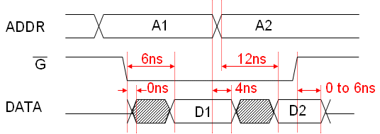 The data sheet specifies that ADDR to DATA is 12ns max, while Gbar to DATA is 6ns.
Since Gbar is delayed 7ns from ADDR, it controls when data appears for the first
access. The timing of DATA for the second access is determined by when the new
address (A2) becomes stable.
The data sheet specifies that ADDR to DATA is 12ns max, while Gbar to DATA is 6ns.
Since Gbar is delayed 7ns from ADDR, it controls when data appears for the first
access. The timing of DATA for the second access is determined by when the new
address (A2) becomes stable.
The "conservative" timing for DATA after Gbar is deasserted depends on the question you're trying to answer. If you're interested in the hold time for DATA after Gbar is deasserted, the data sheet says the minimum time is 0ns. If you're interested in when DATA is tristated (so you can drive it from another chip), the data sheet says the maximum tristate time is 6ns.
-
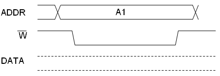
The timing diagram below shows a single WRITE access. Complete the timing diagram,
drawing a detailed plot of the DATA signal showing when it must be valid with respect
to the write enable (Wbar) control signal. Anotate your diagram with times derived
from the data sheet, showing the necessary timing relationships between ADDR, Wbar
and DATA. Assume that the chip's enable signals (E1bar, E2) are asserted and that
the output enable (Gbar) is deasserted.
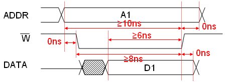 ADDR must be stable for 0ns before Wbar is asserted. Asserting Wbar starts the
write process and the cell to be accessed must be specified before the process begins.
Wbar must be asserted (ie, held low) for at least 8ns assuming Gbar is deasserted.
The "active" edge of Wbar is the low-to-high transition -- that's when the data
is latched in the memory. ADDR must be setup for at least 10ns before the active
edge and DATA must be setup for at least 6ns. Both ADDR and DATA have zero hold time
after the active edge.
ADDR must be stable for 0ns before Wbar is asserted. Asserting Wbar starts the
write process and the cell to be accessed must be specified before the process begins.
Wbar must be asserted (ie, held low) for at least 8ns assuming Gbar is deasserted.
The "active" edge of Wbar is the low-to-high transition -- that's when the data
is latched in the memory. ADDR must be setup for at least 10ns before the active
edge and DATA must be setup for at least 6ns. Both ADDR and DATA have zero hold time
after the active edge.
Problem 2. This problem asks you to design a memory tester that can write to memory and then read these value to validate that they were stored and read back correctly. For this problem you will be using the Motorola MCM6264 8Kx8 static RAM (data sheet). For this problem use four address bit (assume that the higher order address bits are grounded) and four I/O pins (ignore the higher order bits). Your memory tester will write each location with its address. For example, location 4'b0010 will be written with the value 4'b0010. Here's what the test should do:- The tester is started when its RESET input is asserted and then deasserted. You may assume that RESET has already be synchronized with the clock.
- Starting with address 0, write all 16 locations. Location 0 gets the value 4'b0000, location 1 gets the value 4'b0001, and so on.
- Read each location and verify that the correct values were stored and read back. If a mismatch is found, the tester should halt and assert its FAILURE output. If all 16 locations are okay, the test should halt and assert its SUCCESS output.
-
Write a Verilog module that implements the functionality described above. The
modules ports are CLK, RESET, ADDR[3:0], DATA[3:0], Wbar, Gbar, SUCCESS, FAILURE.
You may assume that the memory chip's enables are hardwired to be asserted. Assume
that CLK is driven by a 1.8432Mhz crystal.
You should take care to ensure that the timing relationships between ADDR,
DATA, Wbar and Gbar meet the setup and hold time constraints mentioned in the data sheet.
In particular, note that you'll want to setup the address a cycle before asserting Wbar
and hold for a cycle after deasserting Wbar. It might seem that you could change the
address and assert Wbar in the same cycle (after all the address has to be valid just
when Wbar is asserted). However, different internal delays inside the FPGA might
lead to some address bits changing just after Wbar is asserted, leading to a violation
of the timing.
module test(clk,reset,addr[3:0],data[3:0],wbar,gbar,success,failure);
  input clk,reset;
  output [3:0] addr;    // address for the memory chip
  inout [3:0] data;     // bidirectional data base
  output wbar,gbar,success,failure;

  // we'll use a counter as our state machine.  Each memory access will be
  // allocated 4 cycles.  The address will change at the beginning of the
  // first cycle and be held for all four cycles.  On writes, Wbar will be
  // asserted on the second cycle; DATA will driven with the write data on
  // the second and third cycles.  On reads, Gbar will be asserted on the
  // second and third cycles, and the incoming memory data checked at the
  // end of the second cycle.  All the required timing constraints could
  // be met using only 3 cycles, but, hey, if we make it 4, the counter
  // will serve as our state register and we won't have to fool around with
  // messy next state logic.

  // state[1:0] -- counts through 4 cycles per memory access
  // state[5:2] -- location to be read or written
  // state[6] -- 0 if we're in pass 1 (writing), 1 if we're in pass 2 (reading)
  // state[7] -- 0 if we're running, 1 if we're halted
  reg [7:0] state;

  reg test_failed;  // keeps track of test result

  always @ (posedge clk)
  begin
    if (reset)
      begin state <= 0; test_failed <= 0; end
    else if (!state[7])
      state <= state + 1;   // increment counter if we're still running

    // if we're running in the read phase and this is the end of the second
    // cycle, check to see if the memory is returning the correct data.
    // if not, halt and indicate failure
    if (!state[7] && state[6] && state[1:0]==2'b01 && data!=state[5:2])
      begin state[7] <= 1; test_failed <= 1; end
  end

  // assert memory write enable during write phase on cycle 01
  assign wbar = !(!state[7] && !state[6] && state[1:0]==2'b01);

  // assert memory output enable during read phase on cycles 01 and 10
  assign gbar = !(!state[7] && state[6] && (state[1:0]==2'b01 || state[1:0]==2'b10));

  // memory address comes from the counter
  assign addr = state[5:2];

  // output data to the memory during the write phase on cycles 01 and 10
  wire oe;
  assign oe = !state[7] && !state[6] && (state[1:0]==2'b01 || state[1:0]==2'b10);
  assign data = oe ? state[5:2] : 4'hz;   // this is how we make a tristate output

  // test result indicators -- asserted after test has halted
  assign success = state[7] && !test_failed;
  assign failure = state[7] && test_failed;

endmodule
-
The timing diagram below shows a single WRITE access. Complete the timing diagram,
drawing a detailed plot of the DATA signal showing when it must be valid with respect
to the write enable (Wbar) control signal. Anotate your diagram with times derived
from the data sheet, showing the necessary timing relationships between ADDR, Wbar
and DATA. Assume that the chip's enable signals (E1bar, E2) are asserted and that
the output enable (Gbar) is deasserted.