Problem 1.
The Motorola MCM6264 integrated circuit is a 8Kx8 static RAM. When answering the following
questions about the timing of its various signals please refer to the
data sheet. Assume you are using
the -12 version of the MCM6264.
-
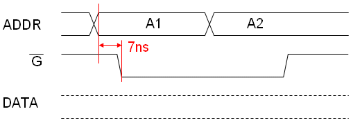
The timing diagram below shows two READ accesses, one for location A1 and the other
for location A2.
Complete the timing diagram, drawing a detailed plot of the DATA signal showing
where it is high impedence, changing and stable. Annotate your diagram with times
derived from the data sheet. Assume that the chip's enable signals (E1bar, E2) are
asserted. Note that the output enable signal (G) goes low 7ns after the address has
become stable. Your timings should reflect that information.
-
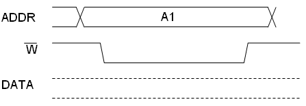
The timing diagram below shows a single WRITE access. Complete the timing diagram,
drawing a detailed plot of the DATA signal showing when it must be valid with respect
to the write enable (Wbar) control signal. Anotate your diagram with times derived
from the data sheet, showing the necessary timing relationships between ADDR, Wbar
and DATA. Assume that the chip's enable signals (E1bar, E2) are asserted and that
the output enable (Gbar) is deasserted.
Problem 2.
This problem asks you to design a memory tester that can write to memory and then
read these value to validate that they were stored and read back correctly. For
this problem you will be using the Motorola MCM6264 8Kx8 static RAM
(
data sheet).
For this problem use four address bit (assume that the higher order address
bits are grounded) and four I/O pins (ignore the higher order bits). Your memory
tester will write each location with its address. For example, location 4'b0010
will be written with the value 4'b0010.
Here's what the test should do:
- The tester is started when its RESET input is asserted and then deasserted. You
may assume that RESET has already be synchronized with the clock.
- Starting with address 0, write all 16 locations. Location 0 gets the value 4'b0000,
location 1 gets the value 4'b0001, and so on.
- Read each location and verify that the correct values were stored and read back.
If a mismatch is found, the tester should halt and assert its FAILURE output. If
all 16 locations are okay, the test should halt and assert its SUCCESS output.
-
Write a Verilog module that implements the functionality described above. The
modules ports are CLK, RESET, ADDR[3:0], DATA[3:0], Wbar, Gbar, SUCCESS, FAILURE.
You may assume that the memory chip's enables are hardwired to be asserted. Assume
that CLK is driven by a 1.8432Mhz crystal.
You should take care to ensure that the timing relationships between ADDR,
DATA, Wbar and Gbar meet the setup and hold time constraints mentioned in the data sheet.
In particular, note that you'll want to setup the address a cycle before asserting Wbar
and hold for a cycle after deasserting Wbar. It might seem that you could change the
address and assert Wbar in the same cycle (after all the address has to be valid just
when Wbar is asserted). However, different internal delays inside the FPGA might
lead to some address bits changing just after Wbar is asserted, leading to a violation
of the timing.