

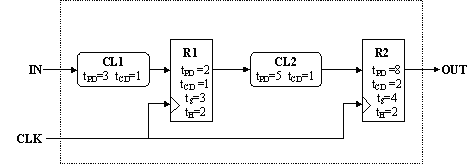
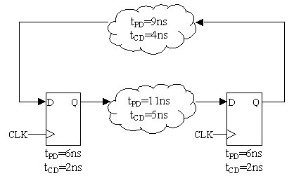
 The components labeled CL1 and CL2 are combinational; R1 and R2 are
D-registers. Timing parameters for each component are
as noted.
The components labeled CL1 and CL2 are combinational; R1 and R2 are
D-registers. Timing parameters for each component are
as noted.

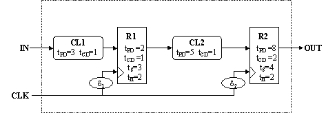
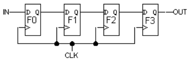 Each of the edge-triggered D flip-flops has a setup time of tS, a
hold time of tH, a propagation delay of tPD and a contamination delay
of tCD. Assume that IN is stable tS before the rising edge of CLK and
tH after the rising edge of CLK.
Each of the edge-triggered D flip-flops has a setup time of tS, a
hold time of tH, a propagation delay of tPD and a contamination delay
of tCD. Assume that IN is stable tS before the rising edge of CLK and
tH after the rising edge of CLK.
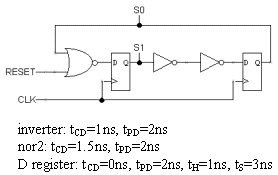
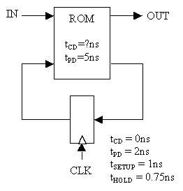
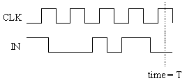 What is the value of OUT at time T?
module divide_by_6(in,out);
  input in;
  output out;

  reg out;
  reg [1:0] count;   // used to count incoming edges

  always @ (posedge in)
  begin
    count <= (count == 2) ? 0 : count+1;  // mod 3 counter
    out <= (count == 2) ? ~ out : out;    // invert OUT every 3 cycles of IN
  end
endmodule
|
|
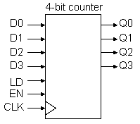
module counter4(clk,d,ld,en,q);
  input clk,ld,en;
  input [3:0] d;
  output [3:0] q;

  reg [3:0] q;

  always @ (posedge clk)
  begin
    q <= ld ? d :    // load counter when LD asserted
         en ? q+1 :  // count when EN asserted
         q;          // otherwise just stay put
  end
endmodule
module counter4_clear(clk,d,ld,en,clr,q);
  input clk,ld,en,clr;
  input [3:0] d;
  output [3:0] q;

  reg [3:0] q;

  // either all items on the sensitivity list are edges
  // or none of the items are edges (can't mix and match!)
  always @ (posedge clr or posedge clk)
  begin
    // asynchronous control signals are implemented with if/case
    //   and they appear on the sensitivity list
    // synchronous control signals appear in computation of q
    //   and they don't appear on the sensitivity list
    if (clr) q <= 0;      // clear takes precedence
    else q <= ld ? d :    // load counter when LD asserted
              en ? q+1 :  // count when EN asserted
              q;          // otherwise just stay put
  end
endmodule
|
| |||||||||||||||||||||||||||||||||||||||||||||||||||||||||||||||
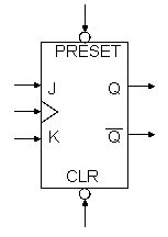
module jkff(clk,j,k,preset_l,clear_l,q,q_l);
  input clk,j,k,preset_l,clear_l;
  output q,q_l;

  reg q;
  assign q_l = ~q;

  // either all items on the sensitivity list are edges
  // or none of the items are edges (can't mix and match!)
  always @ (negedge preset_l or negedge clear_l or posedge clk)
  begin
    // asynchronous control signals are implemented with if/case
    //   and they appear on the sensitivity list
    // synchronous control signals appear in computation of q
    //   and they don't appear on the sensitivity list
    if (!preset_l) q <= 1;       // preset takes precedence
    else if (!clear_l) q <= 0;   // then clear
    else case ({j,k})            // the rest are synchronous operations
      2'b00:  q <= q;            // no change
      2'b10:  q <= 1;            // set
      2'b01:  q <= 0;            // clear
      2'b11:  q <= ~q;           // toggle
    endcase
  end
endmodule
