Problem 1. Consider the following diagram of a simple sequential circuit:
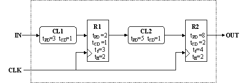 The components labeled CL1 and CL2 are combinational; R1 and R2 are
D-registers. Timing parameters for each component are
as noted.
The components labeled CL1 and CL2 are combinational; R1 and R2 are
D-registers. Timing parameters for each component are
as noted.
-
Write the timing specifications (tS, tH, tCD, tPD, tCLK) for the
system as a whole using the timing specifications for the internal
components that are given in the figure.
It's a good idea to check if the circuit will work for any clock period. We check this by checking if the total contamination delay from R1 to R2 is long enough to cover the hold time of R2. In other words,
-
tH,R2 <= tCD,R1 + tCD,CL2
2 <= 1 + 1
2 <= 2-
tS = tPD,CL1 + tS,R1 = 6, and
tH = tH,R1 - tCD,CL1 = 1.-
tCD = tCD,R2 = 2, and
tPD = tPD,R2 = 8.-
tCLK >= tPD,R1 + tPD,CL2 + tS,R2
tCLK >= 2 + 5 + 4
tCLK >= 11-
Suppose you had available a faster version of CL2 having a propagation
delay of 3 and a contamination delay of zero. Could you substitute
the faster CL2 for the one shown in the diagram? Explain.
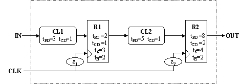
You could not substitute the faster CL2 because our hold time constraint for R2 would not be met. The sum of the contamination delays between R1 and R2 must be greater than the hold time of R2. Using the faster CL2 would reduce the contamination delay sum to 1 which is not greater than the hold time, 2, of R2.We've been treating wires as idealized components that introduce no delay of their own. In the real world, wires have resistance, capacitance and inductance that will cause different frequencies to propagate along the wire at different rates. This means that wires will delay the arrival of sharp rising and falling transitions (which you'll remember from Fourier analysis have signal components at many different frequencies). This effect is particularly bothersome in connection with clock signals since the clock may arrive at separate parts of the circuit at slightly different times. This difference in arrival times of the clock is called clock skew, which we'll model in our simple circuit above as explicit delays along each clock path:
-
Rewrite the timing specifications for the system as a whole taking
into account d1 and d2. Don't make any assumption about the
relative sizes of the two delays.
The delay d1 causes all timing specifications associated with register R1 to be shifted later in time by d1. Likewise the delay d2 causes all timing specifications associated with register R2 to be shifted later in time by d2. Note that we still use the original clock signal as our reference for the system, so the setup times for the registers R1 and R2 become shorter by d1 and d2, respectively, and the hold times for R1 and R2 become longer by d1 and d2. The timing specifications of the system, taking d1 and d2 into account, are:
-
tS = tPD,CL1 + tS,R1 - d1 = 6 - d1
tH = tH,R1 - tCD,CL1 + d1 = 1 + d1
tCD = tCD,R2 + d2 = 2 + d2
tPD = tPD,R2 + d2 = 8 + d2
-
tCLK >= tPD,R1 + tPD,CL2 + tS,R2
tCLK >= 2 + d1 + 5 + 4 - d2
tCLK >= 11 + d1 - d2-
The relative clock skew (d2 - d1) between two registers connected in
a "pipeline" - where the output of the first register is connected,
usually through logic, to the input of the second register - can also
affect the design of a circuit. Explain how relative clock skew
affects the maximum clock frequency of the circuit shown above.
Remember that the relative skew might be positive or negative.
As shown in part (C), tCLK >= 11 - (d2 - d1), rewritten to show the relative clock skew term. One can see that as the relative clock skew becomes positive, the maximum clock frequency increases. Conversely, as the relative clock skew becomes negative, the maximum clock frequency decreases.
-
[Why clock skew keeps integrated circuit designers awake at night.] If
d2 > d1, the circuit shown above will not operate correctly.
Explain why. Will changing the frequency of CLK solve the problem?
Why or why not?
Let's revisit the constraint that the contamination delay from R1 to R2 must cover the hold time of R2:
-
tH,R2 <= tCD,R1 + tCD,logic
2 + d2 <= 1 + d1 + 1
d2 <= d1-
Suggest a way for the designer to change his circuit to guarantee
correct operation given an upper bound, tskew > abs(d2 - d1), on the
maximum relative clock skew. Assume that the timing parameters of the
registers cannot be adjusted.
Adding additional contamination delay, such as a buffer between R1 and R2, will work. This leads to a circuit which has a larger clock period overall.
Problem 2. Consider the following circuit diagram: S0 and S1: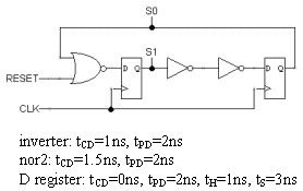
-
What is the smallest clock period for which the circuit still
operates correctly?
There are two contraints to check:
-
tPD,REG + tPD,INV + tPD,INV + tS,REG <= tCLK
tPD,REG + tPD,NOR2 tS,REG <= tCLK-
A sharp-eyed student suggests optimizing the circuit by
removing the pair of inverters and connecting the Q output of the left
register directly to the D input of the right register.
If the clock period could be adjusted appropriately, would the optimized
circuit operate correctly? If yes, explain the adjustment to the clock
period that would be needed.
No, the circuit won't operate correctly since tCD,REG < tHOLD,REG, i.e., the output of the left register doesn't meet the required hold time when connected directly to the input of the right register.
-
When the RESET signal is set to "1" for several cycles, what
values are loaded into the registers? (Give values for S0 and S1.)
S0 = 0, S1 = 0.
-
Assuming the RESET signal has been set to "0" and will stay
that way, what value will with the registers have after the
next clock edge assuming the current values are S0=1 and S1=1?
S0 = 1, S1 = 0.
-
Now suppose there is skew in the CLK signal such that the
rising edge of CLK always arrives at the left register exactly 1ns
before it arrives at the right register. What is the smallest clock
period for which the FSM still operates correctly?
Fortunately the skew doesn't introduce any hold time problems with the input to the right register. tCLK can now be as small as 8ns (both paths between registers fit exactly).
Problem 3. A possible implementation of a sequential circuit with one input and one output is shown below.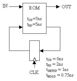
-
What is the smallest value for the ROM's contamination delay
that ensures the necessary timing specifications are met?
tCD,REG + tCD,ROM >= tH,REG, so tCD,ROM >= 0.75ns.
-
Assume that the ROM's tCD = 3ns. What is the smallest clock
period that ensures that the necessary timing specifications are met.
tPD,REG + tPD,ROM + tS,REG = 2 + 5 + 1 = 8ns.
Problem 4. The following schematic has two D-registers and two blocks of combinational logic with the indicated timing specifications. Assume that the registers and that the clock has zero rise and fall time.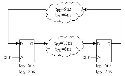
-
Assuming that the clock period is 25ns, what is the maximum setup
time for the registers for which this circuit will operate correctly?
tS <= tCLK - tPD,REG - tPD,LOGIC = 25 - 6 - max(11,9) = 8ns.
-
Assuming that the clock period is 25ns, what is the maximum hold
time for the registers for which this circuit will operate correctly?
tH <= tCD,REG + tCD,LOGIC = 2 + min(4,5) = 6ns.
Problem 5. Use the following circuit in answering the questions below.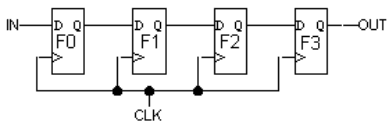 Each of the edge-triggered D flip-flops has a setup time of tS, a
hold time of tH, a propagation delay of tPD and a contamination delay
of tCD. Assume that IN is stable tS before the rising edge of CLK and
tH after the rising edge of CLK.
Each of the edge-triggered D flip-flops has a setup time of tS, a
hold time of tH, a propagation delay of tPD and a contamination delay
of tCD. Assume that IN is stable tS before the rising edge of CLK and
tH after the rising edge of CLK.
-
In order for the circuit shown above to operate correctly what
constraints on tH and tS are necessary? Express them in terms of
tCD, tPD and the clock period.
ensure hold time is met at each register: tH <= tCD
-
What is the minimum clock period at which this circuit can be
clocked and still be guaranteed to work? Express your answer in terms
of tH, tS, tCD and tPD. Assume that timing constraints that do not
depend on the clock period are met.
ensure setup time is met at each register: tPD + tS <= tCLK
-
For just this question suppose there is skew in the CLK signal
such that the rising edge of CLK arrives at the flip-flop labeled F1
1ns before it arrives at the other three flip-flops. Assume that hold
times are not violated. How does this change the minimum clock period
at which the circuit above can be clocked and still be guaranteed to
work?
The minimum clock period increases by 1ns, i.e., we have to have an extra 1ns between clock edges to ensure that the setup time at F1 is met.
-
Consider the following waveform plot for the circuit above. Assume
that IN is stable tS before the rising edge of CLK and tH after the
rising edge of CLK and that time T is more than tPD after the
preceding rising edge of CLK.
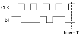 What is the value of OUT at time T?
At time T, OUT = 0 (ie, the value of IN four clock edges earlier).
What is the value of OUT at time T?
At time T, OUT = 0 (ie, the value of IN four clock edges earlier).
Problem 6. Consider the following two waveforms, one of which has 1/6th the frequency of the other.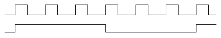
-
Write a Verilog module that takes the top waveform as an input and
produces the bottom waveform as an output.
module divide_by_6(in,out);
  input in;
  output out;

  reg out;
  reg [1:0] count;   // used to count incoming edges

  always @ (posedge in)
  begin
    count <= (count == 2) ? 0 : count+1;  // mod 3 counter
    out <= (count == 2) ? ~ out : out;    // invert OUT every 3 cycles of IN
  end
endmodule
Problem 7. The figure below shows a 4-bit synchronous binary counter: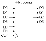
I/O Description D[3:0] 4-bit data input LD when LD is asserted, load D[3:0] into the counter at the next rising edge of CLK EN when EN is asserted, the counter increments by one at the next rising edge of CLK. If LD is asserted, the load takes precedence. CLK clock input Q[3:0] 4-bit counter output -
Write a Verilog module that implements the 4-bit synchronous binary counter.
module counter4(clk,d,ld,en,q); input clk,ld,en; input [3:0] d; output [3:0] q; reg [3:0] q; always @ (posedge clk) begin q <= ld ? d : // load counter when LD asserted en ? q+1 : // count when EN asserted q; // otherwise just stay put end endmodule-
Add an asynchronous clear input, CLR, to your Verilog module. When asserted
it should immediately (not waiting until the next clock edge) set the counter
to 0.
module counter4_clear(clk,d,ld,en,clr,q);
  input clk,ld,en,clr;
  input [3:0] d;
  output [3:0] q;

  reg [3:0] q;

  // either all items on the sensitivity list are edges
  // or none of the items are edges (can't mix and match!)
  always @ (posedge clr or posedge clk)
  begin
    // asynchronous control signals are implemented with if/case
    //   and they appear on the sensitivity list
    // synchronous control signals appear in computation of q
    //   and they don't appear on the sensitivity list
    if (clr) q <= 0;      // clear takes precedence
    else q <= ld ? d :    // load counter when LD asserted
              en ? q+1 :  // count when EN asserted
              q;          // otherwise just stay put
  end
endmodule
Problem 8. The figure and truth table below describe a positive-edge triggered J-K flip-flop with active-low asynchronous preset and clear.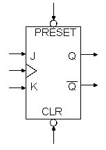
Inputs Outputs preset clear clk J K Q Qbar 0 X X X X 1 0 1 0 X X X 0 1 1 1 no edge X X Q Qbar 1 1 
0 0 Q Qbar 1 1 1 0 1 0 1 1 0 1 0 1 1 1 1 1 toggle -
Write a Verilog module that implements the J-K flip-flop described above.
module jkff(clk,j,k,preset_l,clear_l,q,q_l);
  input clk,j,k,preset_l,clear_l;
  output q,q_l;

  reg q;
  assign q_l = ~q;

  // either all items on the sensitivity list are edges
  // or none of the items are edges (can't mix and match!)
  always @ (negedge preset_l or negedge clear_l or posedge clk)
  begin
    // asynchronous control signals are implemented with if/case
    //   and they appear on the sensitivity list
    // synchronous control signals appear in computation of q
    //   and they don't appear on the sensitivity list
    if (!preset_l) q <= 1;       // preset takes precedence
    else if (!clear_l) q <= 0;   // then clear
    else case ({j,k})            // the rest are synchronous operations
      2'b00:  q <= q;            // no change
      2'b10:  q <= 1;            // set
      2'b01:  q <= 0;            // clear
      2'b11:  q <= ~q;           // toggle
    endcase
  end
endmodule
-
Write a Verilog module that implements the J-K flip-flop described above.
-
Add an asynchronous clear input, CLR, to your Verilog module. When asserted
it should immediately (not waiting until the next clock edge) set the counter
to 0.
-
Write a Verilog module that implements the 4-bit synchronous binary counter.
-
Write a Verilog module that takes the top waveform as an input and
produces the bottom waveform as an output.
-
Consider the following waveform plot for the circuit above. Assume
that IN is stable tS before the rising edge of CLK and tH after the
rising edge of CLK and that time T is more than tPD after the
preceding rising edge of CLK.
-
For just this question suppose there is skew in the CLK signal
such that the rising edge of CLK arrives at the flip-flop labeled F1
1ns before it arrives at the other three flip-flops. Assume that hold
times are not violated. How does this change the minimum clock period
at which the circuit above can be clocked and still be guaranteed to
work?
-
What is the minimum clock period at which this circuit can be
clocked and still be guaranteed to work? Express your answer in terms
of tH, tS, tCD and tPD. Assume that timing constraints that do not
depend on the clock period are met.
-
In order for the circuit shown above to operate correctly what
constraints on tH and tS are necessary? Express them in terms of
tCD, tPD and the clock period.
-
Assuming that the clock period is 25ns, what is the maximum hold
time for the registers for which this circuit will operate correctly?
-
Assuming that the clock period is 25ns, what is the maximum setup
time for the registers for which this circuit will operate correctly?
-
Assume that the ROM's tCD = 3ns. What is the smallest clock
period that ensures that the necessary timing specifications are met.
-
What is the smallest value for the ROM's contamination delay
that ensures the necessary timing specifications are met?
-
Now suppose there is skew in the CLK signal such that the
rising edge of CLK always arrives at the left register exactly 1ns
before it arrives at the right register. What is the smallest clock
period for which the FSM still operates correctly?
-
Assuming the RESET signal has been set to "0" and will stay
that way, what value will with the registers have after the
next clock edge assuming the current values are S0=1 and S1=1?
-
When the RESET signal is set to "1" for several cycles, what
values are loaded into the registers? (Give values for S0 and S1.)
-
A sharp-eyed student suggests optimizing the circuit by
removing the pair of inverters and connecting the Q output of the left
register directly to the D input of the right register.
If the clock period could be adjusted appropriately, would the optimized
circuit operate correctly? If yes, explain the adjustment to the clock
period that would be needed.
-
What is the smallest clock period for which the circuit still
operates correctly?
-
Suggest a way for the designer to change his circuit to guarantee
correct operation given an upper bound, tskew > abs(d2 - d1), on the
maximum relative clock skew. Assume that the timing parameters of the
registers cannot be adjusted.
-
[Why clock skew keeps integrated circuit designers awake at night.] If
d2 > d1, the circuit shown above will not operate correctly.
Explain why. Will changing the frequency of CLK solve the problem?
Why or why not?
-
The relative clock skew (d2 - d1) between two registers connected in
a "pipeline" - where the output of the first register is connected,
usually through logic, to the input of the second register - can also
affect the design of a circuit. Explain how relative clock skew
affects the maximum clock frequency of the circuit shown above.
Remember that the relative skew might be positive or negative.
-
Rewrite the timing specifications for the system as a whole taking
into account d1 and d2. Don't make any assumption about the
relative sizes of the two delays.
-
Suppose you had available a faster version of CL2 having a propagation
delay of 3 and a contamination delay of zero. Could you substitute
the faster CL2 for the one shown in the diagram? Explain.