Problem 1. A certain function F has the following truth table:
A  B  C | F
========|===
0  0  0 | 1
0  0  1 | 0
0  1  0 | 0
0  1  1 | 1
1  0  0 | 1
1  0  1 | 1
1  1  0 | 0
1  1  1 | 1
-
Write a sum-of-products expression for F.
_ _ _ _ _ _ _ F = A*B*C + A*B*C + A*B*C + A*B*C + A*B*C-
Write a minimal sum-of-products expression for F.
Show a combinational circuit that implements F using only
INV and NAND gates.
First construct a Karnaugh map for F:
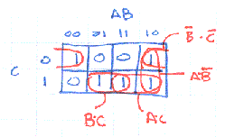 To cover all the 1's in the map we have to use 3 of the 4 patches:
    _ _     _
F = B*C + A*B + B*C
One possible schematic diagram is shown below. Note that the final 3-input NAND gate has been drawn in it's Demorganized form, i.e., an OR gate with inverting inputs.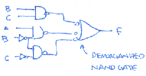
-
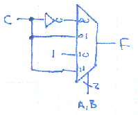
Implement F using one 4-input MUX and inverter.
If we use A and B as the select inputs for the MUX then the four data inputs of the MUX should be tied to one of "0" (ground), "1" (Vdd), "C" or "not C". For this function the following is the correct schematic. Note that by changing the connections on the data inputs we could implement any function of A, B and C.
-
Write a minimal sum-of-products expression for NOT(F).
We can use the Karnaugh map above to answer this question too: just write equations for patches that cover the 0's:
      _   _ _
F = B*C + A*B*C
Problem 2.-
Give a minimal sum-of-products expression that is equivalent
to the follow logic expressions:
    _____
(A) A + B

            _       _ _     _   _     _         _
(B) A*B*C + A*B*C + A*B*C + A*B*C + A*B*C + A*B*C
_ _ (A) A*B (B) B + C-
Multiple choice:
A Karnaugh map can't represent more than 2 variables along a single
dimension because
- Gray code counts can't go beyond 2 bits.
- Each value v along a dimension must be adjacent to all values that are Hamming distance 1 from v.
- Three is not a power of two.
- No reason. You can represent 3 variables along a dimension. You couldn't make 5-variable K-maps otherwise.
2. The 2-bit gray code cycle 00-01-11-10-... handles two variables just fine, but can't be extended to 3 bits. There are 3-bit gray codes but they involve non-adjacent encodings that are Hamming distance 1 apart.-
What is the maximum number of product terms in a minimal
sum-of-products expressions with three variables?
The most complicated K-map that doesn't permit any sort of simplification is a checkerboard of 1's where 50% of the K-map cells can be 1. So in a 3-input K-map, there are eight cells of which four can be 1 in a checkerboard pattern. Each 1 in the checkboard corresponds to a separate product term since it can't be combined with it's neighbors and herefore the maximal number of product terms is 4.
-
True or false: A boolean function of N variables with greater than
2N-1 product terms can always be simplified to an
expression using fewer product terms.
True. If there are more than 2N-1 product terms, the K-map of the function would be more than half full and there would be 1's in at least two adjacent cells, leading to a possible simplification.
-
Suppose the stock room is very low on components and
has only five NAND gates on hand. Would we be able to
build an implementation of any arbitary 2-input boolean
function?
Yes. 3 of the NAND gates could be arranged in a tree, computing the sum-of-products of 2 product terms. (We know from the previous problem that any function with 2 inputs can be simplified down to just 2 product terms.) The other two NAND gates could be used as inverters to produce negations of the inputs which may be needed for the product terms.
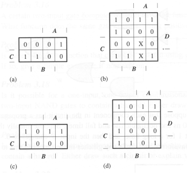
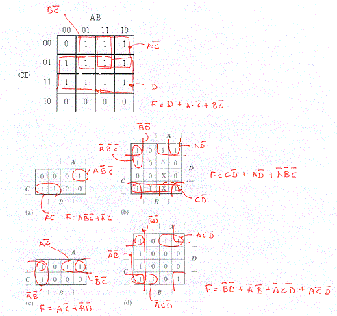
Problem 3. In the Karnaugh maps below the use of "X" in a cell indicates a "don't care" situation where the value of the function for those inputs can be chosen to minimize the size of the overall expression.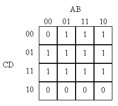
-
Circle the prime implicants in the Karnaugh maps and write a minimal
sum-of-products expression for each of the maps.
Problem 4. The following diagram shows the pulldown circuitry for a static CMOS logic gate that implements the function F(A,B,C,D):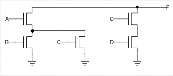
-
Draw a circuit diagram for the pullup circuitry that would complete
the static CMOS implementation of F(A,B,C,D).
-
Assuming the correct pullup circuitry is added to the diagram above,
give a minimal sum-of-products expression for F(A,B,C,D).
     _   _   _   _ _    _ _   _ _   _ _   _ _ _   _ _   _ _   _ _
F = (C + D)*(A + B*C) = A*C + A*D + B*C + B*C*D = A*C + A*D + B*C
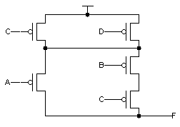
Problem 5. A certain 3-input function G(A,B,C) has the following implementation: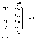
-
Give a minimal sum-of-products expression for G.
    _ _         _
G = A*C + A*C + B
Problem 6. (Katz, problem 4.9) Implement the 2-bit adder function (i.e., 2-bit binary number AB plus 2-bit binary number CD yields a 3-bit result XYZ) using three 8:1 multiplexers.-
Give the truth tables for X, Y and Z.
A B C D | X Y Z
========|======
0 0 0 0 | 0 0 0
0 0 0 1 | 0 0 1
0 0 1 0 | 0 1 0
0 0 1 1 | 0 1 1
0 1 0 0 | 0 0 1
0 1 0 1 | 0 1 0
0 1 1 0 | 0 1 1
0 1 1 1 | 1 0 0
1 0 0 0 | 0 1 0
1 0 0 1 | 0 1 1
1 0 1 0 | 1 0 0
1 0 1 1 | 1 0 1
1 1 0 0 | 0 1 1
1 1 0 1 | 1 0 0
1 1 1 0 | 1 0 1
1 1 1 1 | 1 1 0
-
Show how to implement X, Y, Z using three 8:1 multiplexers. You can
assume you have the constants 0 and 1, the inputs and their complements
available in addition to the multiplexers. Explain how you derived
the inputs to multiplexers.
The selector inputs for the multiplexers are connected to the inputs A, B and C. For a particular value of A, B and C, the corresponding multiplexer data input is connected to
-
0 if the output is 0 for both D = 0 and D = 1
1 if the output is 1 for both D = 0 and D = 1
D if the output is 0 for D = 0 and 1 for D = 1
~D if the output is 1 for D = 0 and 0 for D = 1
          8:1 mux                    8:1 mux                    8:1 mux
        +---------+                +---------+                +---------+
   0 ---|000   out|--- X      0 ---|000   out|--- Y      D ---|000   out|--- Z
   0 ---|001      |           1 ---|001      |           D ---|001      |
   0 ---|010      |           D ---|010      |          ~D ---|010      |
   D ---|011      |          ~D ---|011      |          ~D ---|011      |
   0 ---|100      |           1 ---|100      |           D ---|100      |
   1 ---|101      |           0 ---|101      |           D ---|101      |
   D ---|110      |          ~D ---|110      |          ~D ---|110      |
   1 ---|111      |           D ---|111      |          ~D ---|111      |
        +---------+                +---------+                +---------+
         |||                        |||                        |||
         ABC                        ABC                        ABC
Problem 7. (Katz, problem 4.11) You are working for a company that produces clones of famous name computers. Your assign is to copy the circuit shown below, which is a component of the computer. Because of copyright laws, your boss is very emphatic that the new circuit not resemble the old one. Also, your boss' brother-in-law's electronics wholesale firm has a special deal on multiplexers. So the boss wants you to use only 4:1 multiplexers in your circuit.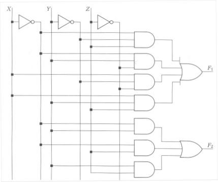
-
Construct a truth table for the circuit above.
X Y Z | F1 F2
======|======
0 0 0 | 0  0
0 0 1 | 1  1
0 1 0 | 1  1
0 1 1 | 0  1
1 0 0 | 1  0
1 0 1 | 0  0
1 1 0 | 0  0
1 1 1 | 1  1
-
Design an implementation using only 4:1 multiplexers, the constants
0 and 1, and the inputs.
          4:1 mux                   4:1 mux                   4:1 mux
        +--------+                +--------+                +--------+
   1 ---|00   out|--- ~Z     Z ---|00   out|--- F1     Z ---|00   out|--- F2
   1 ---|01      |          ~Z ---|01      |           1 ---|01      |
   0 ---|10      |          ~Z ---|10      |           0 ---|10      |
   0 ---|11      |           Z ---|11      |           Z ---|11      |
        +--------+                +--------+                +--------+
         ||                        ||                        ||
         Z0                        XY                        XY
Problem 8. (Katz, problem 4.15a) Consider the following function in sum of products form (not necessarily minimized):_ F(A,B,C,D) = ABC + AD + AC
-
Implement the function F using only an 8:1 multiplexer. You can assume
that you have the constants 0 and 1, and the inputs, but you don't have
their complements (nor inverters to create them!).
We can use the same technique as above. Since we don't have the complements of the inputs available, we'll choose a variable that only appears in positive form as the variable to hook to the data inputs of the mux (ie, B, C or D).
          8:1 mux
        +---------+
   0 ---|000   out|--- F(A,B,C,D)
   0 ---|001      |
   0 ---|010      |
   1 ---|011      |
   D ---|100      |
   1 ---|101      |
   D ---|110      |
   1 ---|111      |
        +---------+
         |||
         ABC
Problem 9. (Katz, problem 4.22) You are to implement a combinational multiplier. It has two 2-bit inputs and a 4-bit output. The first 2-bit input is represented by the variables A, B; the second 2-bit input is represented by C, D. The outputs are W, X, Y, Z, from the most significant bit to the least.-
Complete a truth table that describes the functional behavior of the multiplier.
A B C D | W X Y Z
========|========
0 0 0 0 | 0 0 0 0    0 * 0 = 0
0 0 0 1 | 0 0 0 0    0 * 1 = 0
0 0 1 0 | 0 0 0 0    0 * 2 = 0
0 0 1 1 | 0 0 0 0    0 * 3 = 0
0 1 0 0 | 0 0 0 0    1 * 0 = 0
0 1 0 1 | 0 0 0 1    1 * 1 = 1
0 1 1 0 | 0 0 1 0    1 * 2 = 2
0 1 1 1 | 0 0 1 1    1 * 3 = 3
1 0 0 0 | 0 0 0 0    2 * 0 = 0
1 0 0 1 | 0 0 1 0    2 * 1 = 1
1 0 1 0 | 0 1 0 0    2 * 2 = 4
1 0 1 1 | 0 1 1 0    2 * 3 = 6
1 1 0 0 | 0 0 0 0    3 * 0 = 0
1 1 0 1 | 0 0 1 1    3 * 1 = 1
1 1 1 0 | 0 1 1 0    3 * 2 = 6
1 1 1 1 | 1 0 0 1    3 * 3 = 9
-
Find the minimum sum of products forms for the outputs using Karnaugh maps.
W AB 00 01 11 10 CD 00 0 0 0 0 01 0 0 0 0 11 0 0 1 0 10 0 0 0 0 W = ABCD
X AB 00 01 11 10 CD 00 0 0 0 0 01 0 0 0 0 11 0 0 0 1 10 0 0 1 1 _ _ X = ACD + ABC
Y AB 00 01 11 10 CD 00 0 0 0 0 01 0 0 1 1 11 0 1 0 1 10 0 1 1 0 _ _ _ _ Y = ACD + ABD + ABC + BCD
Z AB 00 01 11 10 CD 00 0 0 0 0 01 0 1 1 0 11 0 1 1 0 10 0 0 0 0 Z = BD
Problem 10. (Katz, problem 4.23) An n-input majority fnction asserts its output whenever more than half of its inputs are asserted. You are to implement a seven-input majority function, which will assert its output whnever four or more of its inputs are asserted. Don't panic just because this is a seven-variable function. Build it up as multilevel function whose subfunctions each have less than six variables. As a block diagram, it looks like the figure below. Circuits #1 and #2 tally the number of the inputs that are asserted, providing the count in binaryon the outputs (V,Y are the most significant bits; W,Z are the least significant bits). Based on these second-level inputs, Q determines if more than four or more of the original inputs are 1.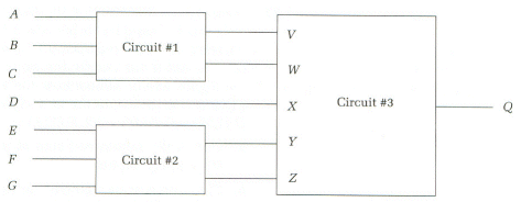
-
Find the minimized sum of products for circuit #1 (circuit #2 is
identical). The functions V and W should look familiar. What do
they implement?
Circuits #1 and #2 are full adders: they sum their three inputs to produce a 2-bit result. The minimal sum of products is
V = AB + BC + AC (full adder carry out) __ _ _ __ W = ABC + ABC + ABC + ABC (full adder sum out)-
Complete the 5-variable truth table for circuit #3.
Q is 1 if at least 4 of the 7 inputs are one.
V W X Y Z | Q
=============
0 0 0 0 0 | 0
0 0 0 0 1 | 0
0 0 0 1 0 | 0
0 0 0 1 1 | 0
0 0 1 0 0 | 0
0 0 1 0 1 | 0
0 0 1 1 0 | 0
0 0 1 1 1 | 1
0 1 0 0 0 | 0
0 1 0 0 1 | 0
0 1 0 1 0 | 0
0 1 0 1 1 | 1
0 1 1 0 0 | 0
0 1 1 0 1 | 0
0 1 1 1 0 | 1
0 1 1 1 1 | 1
1 0 0 0 0 | 0
1 0 0 0 1 | 0
1 0 0 1 0 | 1
1 0 0 1 1 | 1
1 0 1 0 0 | 0
1 0 1 0 1 | 1
1 0 1 1 0 | 1
1 0 1 1 1 | 1
1 1 0 0 0 | 0
1 1 0 0 1 | 1
1 1 0 1 0 | 1
1 1 0 1 1 | 1
1 1 1 0 0 | 1
1 1 1 0 1 | 1
1 1 1 1 0 | 1
1 1 1 1 1 | 1
-
Find the minimum sum of products form for Q using
the Karnaugh map method. Hint: extend a 4-variable
Karnaugh map into the third dimension.
We'll use the third dimension for the variable X. In each cell of the table below, we'll write <value when X=1>:<value when X=0>
Q VW 00 01 11 10 YZ 00 0:0 0:0 1:0 0:0 01 0:0 0:0 1:1 1:0 11 1:0 1:1 1:1 1:1 10 0:0 1:0 1:1 1:1 Q = VY + XYZ + XVW + XYW + XVZ + WYZ + VWZ
Problem 11. Digital Widgets Co. has introduced a new logic IC consisting of two comparator cells in a 14-pin package. A comparator cell, as drawn below, has four inputs and two outputs.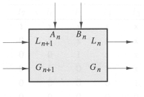 The inputs are labeled An, Bn, Gn+1, and Ln+1, and the outputs are
labeled Gn and Ln. The G and L signals have the meanings "A greater
than B" and "A less than B," respectively. If both G and L are false,
the meaning is A = B. G and L are never both true. Two k-bit numbers
A and B may be compared using a circuit such as the following:
The inputs are labeled An, Bn, Gn+1, and Ln+1, and the outputs are
labeled Gn and Ln. The G and L signals have the meanings "A greater
than B" and "A less than B," respectively. If both G and L are false,
the meaning is A = B. G and L are never both true. Two k-bit numbers
A and B may be compared using a circuit such as the following:
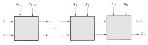 The most significant bits are supplied as Ak-1 and
Bk-1, and the least significant bits are A0 and B0.
The output of a comparison is taken from the G and L outputs of the
lowest-order cell (G0 and L0). Gn+1 and Ln+1 of the highest-order
cell are connected to logical 0 to indicate that the numbers are
assumed to be equal until some difference is found between a pair of
bits Ai and Bi.
If the Gn+1 and Ln+1 inputs indicate that higher-order bits have
established A > B or A < B, then cell n must propagate that
result to Gn and Ln. However, if Gn+1 and Ln+1 indicate that the
higher-order bits are equal, then cell n must compare its bit of A and
B to determine if A > B, A < B, or A = B and must signal that
result appropriately at Gn and Ln.
The most significant bits are supplied as Ak-1 and
Bk-1, and the least significant bits are A0 and B0.
The output of a comparison is taken from the G and L outputs of the
lowest-order cell (G0 and L0). Gn+1 and Ln+1 of the highest-order
cell are connected to logical 0 to indicate that the numbers are
assumed to be equal until some difference is found between a pair of
bits Ai and Bi.
If the Gn+1 and Ln+1 inputs indicate that higher-order bits have
established A > B or A < B, then cell n must propagate that
result to Gn and Ln. However, if Gn+1 and Ln+1 indicate that the
higher-order bits are equal, then cell n must compare its bit of A and
B to determine if A > B, A < B, or A = B and must signal that
result appropriately at Gn and Ln.
-
Draw a logic diagram for an implementation of the Digital Widgets
comparator cell.
The equations for Gn and Ln are
            ____    __
Gn = Gn+1 + Ln+1*An*Bn
            ____ __
Ln = Ln+1 + Gn+1*An*Bn
If we construct a schematic using INV, AND and OR, the resulting circuit would have a Tpd of 3 gate delays.-
Since there is delay associated with the propagation of the G and L
signals through each cell, we could make the comparator work faster
by redesigning the basic cell to compare two bits at a time, halving the number
of stages through which the G and L signals will need to propagate.
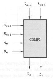 Work out expressions for Gn and Ln as functions of Gn+2, Ln+2,
An+1, Bn+1, An, and Bn. Express your answers in the form
Work out expressions for Gn and Ln as functions of Gn+2, Ln+2,
An+1, Bn+1, An, and Bn. Express your answers in the form
____ ____ ____ ____ __ Gn = Gn+2 + Ln+2*(An+1*Bn+1 + (An+1*Bn+1 + An+1*Bn+1)*An*Bn) ____ ____ ____ ____ __ Ln = Ln+2 + Gn+2*(An+1*Bn+1 + (An+1*Bn+1 + An+1*Bn+1)*An*Bn)-
Given a reasonable implementation of the equations for Gn and Ln
derived in part B, how does the delay from a change in Gn+2
and Ln+2 to the appearance of correct outputs at Gn
and Ln compare with the corresponding delay for a circuit composed
of a cascade of two of the cells developed in part A?
Assume that all A and B inputs remain unchanged throughout.
Note: The reason for our interest in the propagation delay of the G and
L signals, specifically, is that in a chain of N comparators, every
extra gate delay in the G--L path will penalize total performance by N
gate delays. The time it takes for a change in an A or B input to be reflected
in the corresponding G or L output is also important, but improvements here
can at best result in decreasing total delay by some constant amount.
If we expand out either equation for the two-bit-at-a-time cell, we end up with 4 product terms, two of which involve 5 inputs. If we have 5-input gates in our library, we can implement the two-bit cell with the same Tpd as the one-bit cell. So Gn and Ln are produced by a two-bit cell with half the delay as from a cascade of two one-bit cells. If we restrict ourselves to 4-input gates, this adds one gate delay to Tpd for the two-bit cell (Tpd = 4), still an improvement over two one-bit cells (Tpd = 6).
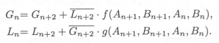
Problem 12. The Xilinx 4000 series field-programmable gate array (FPGA) can be programmed to emulate a circuit made up of many thousands of gates; for example, the XC4025E can emulate circuits with up to 25,000 gates. The heart of the FPGA architecture is a configurable logic block (CLB) which has a combinational logic subsection with the following circuit diagram: There are two 4-input function generators and one 3-input function
generator, each capable of implementing an arbitrary Boolean function
of its inputs.
The function generators are actually small 16-by-1 and 8-by-1
memories that are used as lookup tables; when the Xilinx device is
"programmed" these memories are filled with the appropriate values so
that each generator produces the desired outputs. The multiplexer
select signals (labeled "Mx" in the diagram) are also set by the
programming process to configure the CLB. After programming, these Mx
signals remain constant during CLB operation.
The following is a list of the possible configurations. For each
configuration indicate how each the control signals should be
programmed, which of the input lines (C1-C4, F1-F4, and G1-G4) are
used, and what output lines (X, Y, or Z) the result(s) appear on.
There are two 4-input function generators and one 3-input function
generator, each capable of implementing an arbitrary Boolean function
of its inputs.
The function generators are actually small 16-by-1 and 8-by-1
memories that are used as lookup tables; when the Xilinx device is
"programmed" these memories are filled with the appropriate values so
that each generator produces the desired outputs. The multiplexer
select signals (labeled "Mx" in the diagram) are also set by the
programming process to configure the CLB. After programming, these Mx
signals remain constant during CLB operation.
The following is a list of the possible configurations. For each
configuration indicate how each the control signals should be
programmed, which of the input lines (C1-C4, F1-F4, and G1-G4) are
used, and what output lines (X, Y, or Z) the result(s) appear on.
-
An arbitrary function F of up to four input variables, plus another
arbitrary function G of up to four unrelated input variables, plus a
third arbitrary function H of up to three unrelated input variables.
Let X = F(F1, F2, F3, F4), Z = G(G1, G2, G3, G4), Y = H(C1, C2, C3). The necessary control signals are:
-
MA = 1
MB = 1
MC = 0 (select C1)
MD = 1 (select C2)
ME = 2 (select C3)-
An arbitrary single function of five variables.
Let Y = F(A1, A2, A3, A4, A5). This can be implemented using both 4-input logic functions, and selecting between the two outputs with the 3-input logic function.
-
Z=f(A1, A2, A3, A4, 0),
X=f(A1, A2, A3, A4, 1),
Y= Z if A5=0, else Y=X-
MA = 0
MB = 0
MC = X (value doesn't matter)
MD = X (value doesn't matter)
ME = 0 (select C1)-
An arbitrary function of four variables together with some functions
of six variables. Characterize the functions of six variables that
can be implemented.
Let Z = G(G1, G2, G3, G4) - any function of 4 variables.
-
X = F(F1, F2, F3, F4)
Y = H(C1, C2, X) = H(C1, C2, F(F1, F2, F3, F4))-
MA = 0
MB = 1
MC = X (value doesn't matter)
MD = 0 (select C1)
ME = 1 (select C2)-
Some functions of up to nine variables. Characterize the functions of
up to nine variables that can be implemented.
Let
-
X = F(F1, F2, F3, F4)
Z = G(G1, G2, G3, G4)
Y = H(C1, X, Z) = H(C1, F(F1, F2, F3, F4), G(G1, G2, G3, G4))
-
MA = 0
MB = 0
MC = X (value doesn't matter)
MD = X (value doesn't matter)
ME = 0 (select C1)
-
[Optional challenge] Can every function of six inputs be implemented?
If so, explain how. If not, give a 6-input function and explain why
it can't be implemented in the CLB.
The functions of 6 variables which we can implement must be of the form
-
Y = y(C1, C2, f(F1,F2,F3,F4))
-
Y = y(C1, f(F1, F2, F3, F4), g(G1, G2, G3, G4))
-
Y = A1A2A3A4A5 + A1A2A3A4A6 + A1A2A3A5A6 + A1A2A4A5A6
+ A1A3A4A5A6 +A2A3A4A5A6
-
[Optional challenge] Can every function of six inputs be implemented?
If so, explain how. If not, give a 6-input function and explain why
it can't be implemented in the CLB.
-
Some functions of up to nine variables. Characterize the functions of
up to nine variables that can be implemented.
-
An arbitrary function of four variables together with some functions
of six variables. Characterize the functions of six variables that
can be implemented.
-
An arbitrary single function of five variables.
-
An arbitrary function F of up to four input variables, plus another
arbitrary function G of up to four unrelated input variables, plus a
third arbitrary function H of up to three unrelated input variables.
-
Given a reasonable implementation of the equations for Gn and Ln
derived in part B, how does the delay from a change in Gn+2
and Ln+2 to the appearance of correct outputs at Gn
and Ln compare with the corresponding delay for a circuit composed
of a cascade of two of the cells developed in part A?
Assume that all A and B inputs remain unchanged throughout.
Note: The reason for our interest in the propagation delay of the G and
L signals, specifically, is that in a chain of N comparators, every
extra gate delay in the G--L path will penalize total performance by N
gate delays. The time it takes for a change in an A or B input to be reflected
in the corresponding G or L output is also important, but improvements here
can at best result in decreasing total delay by some constant amount.
-
Since there is delay associated with the propagation of the G and L
signals through each cell, we could make the comparator work faster
by redesigning the basic cell to compare two bits at a time, halving the number
of stages through which the G and L signals will need to propagate.
-
Draw a logic diagram for an implementation of the Digital Widgets
comparator cell.
-
Find the minimum sum of products form for Q using
the Karnaugh map method. Hint: extend a 4-variable
Karnaugh map into the third dimension.
-
Complete the 5-variable truth table for circuit #3.
-
Find the minimized sum of products for circuit #1 (circuit #2 is
identical). The functions V and W should look familiar. What do
they implement?
-
Find the minimum sum of products forms for the outputs using Karnaugh maps.
-
Complete a truth table that describes the functional behavior of the multiplier.
-
Implement the function F using only an 8:1 multiplexer. You can assume
that you have the constants 0 and 1, and the inputs, but you don't have
their complements (nor inverters to create them!).
-
Design an implementation using only 4:1 multiplexers, the constants
0 and 1, and the inputs.
-
Construct a truth table for the circuit above.
-
Show how to implement X, Y, Z using three 8:1 multiplexers. You can
assume you have the constants 0 and 1, the inputs and their complements
available in addition to the multiplexers. Explain how you derived
the inputs to multiplexers.
-
Give the truth tables for X, Y and Z.
-
Give a minimal sum-of-products expression for G.
-
Assuming the correct pullup circuitry is added to the diagram above,
give a minimal sum-of-products expression for F(A,B,C,D).
-
Draw a circuit diagram for the pullup circuitry that would complete
the static CMOS implementation of F(A,B,C,D).
-
Circle the prime implicants in the Karnaugh maps and write a minimal
sum-of-products expression for each of the maps.
-
Suppose the stock room is very low on components and
has only five NAND gates on hand. Would we be able to
build an implementation of any arbitary 2-input boolean
function?
-
True or false: A boolean function of N variables with greater than
2N-1 product terms can always be simplified to an
expression using fewer product terms.
-
Multiple choice:
A Karnaugh map can't represent more than 2 variables along a single
dimension because
-
Give a minimal sum-of-products expression that is equivalent
to the follow logic expressions:
-
Write a minimal sum-of-products expression for NOT(F).
-
Implement F using one 4-input MUX and inverter.
-
Write a minimal sum-of-products expression for F.
Show a combinational circuit that implements F using only
INV and NAND gates.