Beta quickies: Discussed in section In an unpipelined Beta implementation, when is the signal RA2SEL set to "1"? The RA2SEL signal is set to 1 when executing a ST instruction. When RA2SEL is 1 the 5-bit Rc field of the instruction is sent to the RA2 port of the register file, causing Reg[Rc] to be sent to the write data port of main memory. Discussed in section In an unpipelined Beta implementation, when executing a BR(foo,LP) instruction to call procedure foo, what should WDSEL should be set to? BR(foo,LP) == BEQ(R31,foo,LP). All BNE/BEQ instructions save the address of the following instruction in the specified destination register (LP in the example instruction). So WDSEL should be set 0, selecting the output of the PC+4 logic as the data to be written into the register file. Discussed in section The minimum clock period of the unpipelined Beta implementation is determined by the propagation delays of the data path elements and the amount of time it takes for the control signals to become valid. Which of the following select signals should become valid first in order to ensure the smallest possible clock period: PCSEL, RA2SEL, ASEL, BSEL, WDSEL, WASEL? To ensure the smallest possible clock period RA2SEL should become valid first. The RA2SEL mux must produce a stable register address before the register file can do its thing. All other control signals affect logic that operates after the required register values have been accessed, so they don't have to be valid until later in the cycle. Notta Kalew, a somewhat fumble-fingered lab assistant, has deleted the opcode field from the following table describing the control logic of an unpipelined Beta processor.

Discussed in section Help Notta out by identifying which Beta instruction is implemented by each row of the table. Row 1: SUBC
Row 2: BEQ
Row 3: LDR
Row 4: CMPEQ
Row 5: ST
Discussed in section Notta notices that WASEL is always zero in this table. Explain briefly under what circumstances WASEL would be non-zero. WASEL is 1 if an interrupt is being serviced, an illegal opcode is trapped, or a fault occurs. When WASEL is 1, it selects XP as the write address for the register file; Reg[XP] is where we store the current PC+4 whenever there is an interrupt, a fault, or an illegal opcode. Discussed in section Notta has noticed the following C code fragment appears frequently in the benchmarks:

   int *p;     /* Pointer to integer array */
   int i,j;    /* integer variables */
   ...
   j = p[i];   /* access ith element of array */

The pointer variable p contains the address of a dynamically allocated array of integers. The value of p[i] is stored at the address Mem[p]+4*Mem[i] where p and i are locations containing the values of the corresponding C variables. On a conventional Beta this code fragment is translated to the following instruction sequence:

   LD(...,R1)     /* R1 contains p, the array base address */
   LD(...,R2)     /* R2 contains I, the array index */
   ...
   SHLC(R2,2,R0)  /* compute byte-addressed offset = 4*i */
   ADD(R1,R0,R0)  /* address of indexed element */
   LD(R0,0,R3)    /* fetch p[i] into R3 */

Notta proposes the addition of an LDX instruction that shortens the last three instructions to

   SHLC(R2,2,R0)  /* compute byte-addressed offset = 4*i */
   LDX(R0,R1,R3)  /* fetch p[i] into R3 */

Give a register-transfer language description for the LDX instruction. Examples of register-transfer language descriptions can be for other Beta instructions in the Beta Documentation handed out in lecture.

LDX( Ra, Rb, Rc )
    EA <- Reg[Ra] + Reg[Rb]
    Reg[Rc] <- Mem[EA]
    PC <- PC + 4
Discussed in section Using a table like the one above specify the control signals for the LDX opcode.
         LDX
ALUFN    "+"
WERF     1
BSEL     0
WDSEL    2
WR       0
RA2SEL   0
PCSEL    0
ASEL     0
WASEL    0
It occurs to Notta that adding an STX instruction would probably be useful too. Using this new instruction, p[i] = j might compile into the following instruction sequence:
   SHLC(R2,2,R0)  /* compute byte-addressed offset = 4*i */
   STX(R3,R0,R1)  /* R3 contains j, R1 contains p */

Briefly describe what modifications to the Beta datapath would be necessary to be able to execute STX in a single cycle. The register transfer language description of STX would be:

STX(Rc, Rb, Ra)
    EA <- Reg[Ra] + Reg[Rb]
    Mem[EA] <- Reg[Rc]
    PC <- PC + 4
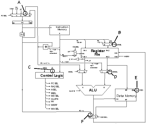
It's evident that we need to perform 3 register reads, but the Beta's register file has only 2 read ports. Thus we need to add a third read port to the register file.

Incidentally, adding a third read port would eliminate the need for the RA2SEL mux because we no longer need to choose between Rb and Rc, since each register field has its own read port. One Beta manufacturer is having quality-control problems with their design. In particular, they've had reliability issues with various device connections that are circled in the attached diagram.

Your job is to write some test programs to help determine if a machine is fault-free. Assume that when a device connection is "faulty," the indicated bus or signal is always "stuck-at 0" instead of the expected value. For each of the circled connections, write an instruction sequence that when executed for a specified number of cycles would indicate whether the connection was okay by leaving a "1" in R0 and leaves some other value in R0 if the connection was faulty. You can assume that all registers are reliably set to 0 before each sequence is executed.

Give your instruction sequence for each of the six indicated faults and briefly explain how each sequence detects the fault and produces something besides "1" in R0 when the fault is present.

Discussed in section Fault A: Input 1 of PCSEL mux stuck at 0.

      . = 0
      BEQ(R0,.+4,R31)
      ADDC(R0,1,R0)
Execute for 2 cycles. If fault A is not present, R0 contains 1 after the second cycle. If fault A is present, the second instruction is fetched from location 0 (instead of 4), so the value of R0 stays 0.
Discussed in section Fault B: RA2SEL mux control signal stuck at 0.
      . = 0
      ADDC(R1,1,R1)
      ST(R1,0,R0)
      LD(R0,0,R0)
Execute for 3 cycles. If fault B is not present, the ST instruction writes the value 1 into location 0, which is then LDed into R0. If fault B is present, the ST instruction writes the contents of R0 instead (ie, the value 0), so now the LD instruction puts 0 into R0.
Discussed in section Fault C: Z input to control logic stuck at 0.
      . = 0
      BNE(R0,.+8,R31)
      ADDC(R0,1,R0)
Execute for 2 cycles. If fault C is not present, R0 is incremented to 1 since the branch is not taken. If fault C is present, the BNE instruction always branches, skipping over the ADDC instruction and leaving the contents of R0 unchanged (ie, it's still 0).
Fault D: BSEL mux control signal stuck at 0.
      . = 0
      ADDC(R0,1,R0)
Execute for 1 cycle. If fault D is not present, R0 is increment to 1. If fault D is present, the high-order 5-bits of the literal field (i.e., where Rb is encoded) is used as a register address, and the contents of that register is added to R0. Since the literal is "1", the second register is R0 (containing 0), so the value written into R0 is 0.
Fault E: WR memory control signal stuck at 0.
      . = 0
      ADDC(R1,1,R1)
      ST(R1,X,R31)
      LD(R31,X,R0)

      . = 0x100
X:    LONG(0)
Execute for 3 cycles. If fault E is not present, the ST instruction writes the value 1 into X, which is then LDed into R0. If fault B is present, the ST instruction has no effect, so now the LD instruction loads the original value of location X into R0.
Fault F: Input 0 of WDSEL mux stuck at 0.
      . = 0
      BEQ(R0,.+4,R1)
      SUBC(R1,3,R0)
Execute for 2 cycles. If fault F is not present, the BEQ instruction loads 4 into R1 and the SUBC loads 1 into R0. If fault F is present, the BEQ instruction load 0 into R0 and the SUBC loads -3 into R0.
Flaky Beta's, Inc. has an interesting business plan: they buy -- very cheaply -- Beta processors manufactured by other companies with slight defects and market them as implementing "variants" of the Beta Instruction Set Architecture. FBI's plan is simply to change the documentation of the instructions affected by the manufacturing flaws in each machine, presuming that its customers can live with the revised machine behavior.

The FB1 and FB2 are based on a non-pipelined Beta. They perform exactly as a fully functional non- pipelined Beta (see diagrams at the end of the quiz), except for the following flaws:

Note that, aside from the above flaws, the defective processors behave identically to their fully-functional counterparts; control signals, for example, are generated as for a working Beta processor.

FBI tests both the FB1 and FB2 on six Beta instructions: LDR, ST, SUBC, BNE, LD and JMP. They find that each of the flaws affects only one of the six instructions. Which Beta instructions does the FB1 flaw affect? Which Beta instructions are affected by FB2 flaw? FB1 flaw: ASEL is nonzero only when executing the LDR instruction.

FB2 flaw: RA2SEL is nonzero only when executing the ST instruction. Of course many programs use all the instructions in the Beta ISA, so clients need to know if it is possible to rewrite their programs so that they perform the same computation whether they run on an unflawed Beta or an FBI processor. It's okay if the rewritten program takes a different number of instructions than the original. When answering the questions below, assume that rewritten programs still fit in the available memory.

Is it possible to rewrite an arbitrary program so that it will perform correctly on both an unflawed Beta and an FB1? Yes. We've seen several ways of using a sequence of operations to load a 32-bit constant into a register. For example:

.macro LDR(label,RX) {
    BR(.+8,RX)    | load address of following word into RX
    LONG(label)   | address of constant to be loaded
    LD(RX,0,RX)   | load address into register
    LD(RX,0,RX)   | load constant into register
}
Is it possible to rewrite an arbitrary program so that it will perform correctly on both an unflawed Beta and an FB2? Yes, although it's a bit tricky. You have to rewrite the program so that all stores into memory have the form ST(R0,0,Rx), i.e., where Rx contains the address of the memory location to be written and R0 contains the write data. In an unflawed Beta, the RA2SEL mux would select the Rc field of the ST (R0 = 0b00000). In an FB2, the hardware selects the Rb field instead, but if the literal field is zero, then the Rb field is also 0. In either case the contents of R0 are read from the register file and sent to the memory.
A 6.004 student, Pete Coshaver, has suggested the following modified Beta design to minimize the critical path in his unpipelined implementation.

Briefly describe the differences between the modified Beta shown above and the Beta described in lecture. 1) The ASEL mux has moved from the A-input to the ALU into the address path for main memory.

2) The 3-input WDSEL mux has been split into two cascaded 2-input muxes. Which instructions have their critical path reduced as a result of Pete's modifications? The critical path for the LDR instruction is reduced since the address no longer has to pass through the ALU before being sent to main memory.

Assuming that tPD of a 2-input mux is smaller than tPD of a 3-input mux, the critical path for the LD instruction would also be reduced. On a given instruction Pete's control logic generates the following control signals. What is the most likely opcode of instruction being executed?

PCSEL	0
RA2SEL	-
BSEL	1
ALUFN	+
Wr	0
WERF	1
WASEL	0
AdrSEL	0
WDSEL1	1
WDSEL0	-
The operation performed is Reg[Rc] = Mem[Reg[Ra] + sxt(literal)] which is the specification for the LD instruction. The key was noticing that WDSEL1 = 1, selecting the output of main memory as the source of data to be written into the register file. What impact does Pete's redesign of the write-data-select multiplexer (controlled by the WDSEL0 and WDSEL1 control lines) have on the original Beta design?
  1. Pete's old Beta control ROM will not work with his modified Beta design
  2. It requires the BOOL unit of the ALU to be redesigned.
  3. It is most likely slower than the 3-input multiplexer used in the original Beta.
  4. It has no impact; it is functionally identical to the original design.
  5. Some standard Beta instructions can no longer be implemented with Pete's changes.
d. Surprisingly it has no impact since none of the control signal settings has to change (even the original WDSEL encoding still works!).
What is the most appropriate setting of the WDSEL0 and WDSEL1 control lines when executing a BEQ instruction? WDSEL0 = 0 and WDSEL1 = 0, selecting the output of the PC+4 as the data to be written into the register file. Pete would like to connect the ASEL signal of his old Beta design to the AdrSEL signal in his new design. For what Beta instruction type is it necessary for Pete to change the contents of his control ROM before his modified Beta will behave identical to the original version? No modifications are necessary. ASEL = 0 except when executing the LDR instruction, just like the original Beta. Pete was also able to reduce the size of his control logic by merging the functions of two signals into a single output signal. What two signals, from the list given below, could he have merged?
    a) WDSEL0 and WDSEL1
    b) WDSEL0 and WERF
    c) AdrSEL and WASEL
    d) BSEL and RA2SEL
    e) AdrSEL and WR
A look at the control logic chart for the Beta reveals that BSEL and RA2SEL are the same if we choose appropriate values for the "don't care" entries for RA2SEL.
The minimum clock period of Pete's unpipelined Beta implementation is determined by the propagation delays of the data path elements and the amount of time it takes for the control signals to become valid. Which select signal(s) should become valid first in order to ensure the smallest possible clock period? As in the original Beta, RA2SEL should become valid first so that the register file can get started on fetching register values. The other control signals control logic that operates after the register reads are complete.
Consider the following potential additions to the Beta Instruction set:
	// Swap register contents with memory location
	MSWP (Ra, literal, Rc)
		PC <- PC + 4
		EA <- Reg[Ra] + SEXT(literal)
		tmp <- Mem[EA]
		Mem[EA] <- Reg[Rc]
		Reg[Rc] <- tmp

	// Move if zero
	MVZ (Ra, Rb, Rc)
		PC <- PC + 4
		if Reg[Ra] = 0 then Reg[Rc] <- Reg[Rb]

	// Move constant if zero
	MVZC (Ra, literal, Rc)
		PC <- PC + 4
		if Reg[Ra] = 0 then Reg[Rc] <- SEXT(literal)
Specify the control signals configurations needed to execute these instructions on an unpipelined Beta.
         MSWP  MVZ    MVZC
ALUFN    "+"   "B"    "B"
WERF     1     Z?1:0  Z?1:0
BSEL     1     0      1
WDSEL    2     1      1
WR       1     0      0
RA2SEL   1     0      -
PCSEL    0     0      0
ASEL     0     -      -
WASEL    0     0      0
Explain why the following instructions cannot be added to our Beta instruction set without further modifications:

	// Push Rc onto stack pointed to by Ra
	PUSH(Rc, 4, Ra)
		PC <- PC + 4
		Mem[Reg[Ra]] <- Reg[Rc]
		Reg[Ra] <- Reg[Ra] + 4

	// Store indexed (base + index register)
	STX(Ra, Rb, Rc)
		PC <- PC + 4
		Mem[Reg[Ra] + Reg[Rb]] <- Reg[Rc]
To implement PUSH, the ALU would have to produce two values: Reg[Ra] to be used as the memory address and Reg[Ra]+4 to be written into the register file.

To implement STX, the Beta has to read three registers, but it only has two read ports on the register file.