Consider the following circuit that implements the 2-input function H(A,B):

Discussed in section Fill in the following truth table for H:

ABH
00 
01 
10 
11 
ABH
001
011
100
111
Discussed in section Give a sum-of-products expression that corresponds to the truth table above. The equation has one product term for each line of the truth table where H(A,B) = 1. Each product term contains two literals, one for each of the two inputs.
    _ _         _
H = A*B + A*B + A*B
Discussed in section Using the following table of timing specifications for each component, what are tCD, tPD and tR for the circuit shown above?

gatetCDtPDtRtF
I3ps15ps8ps5ps
ND25ps30ps11ps7ps
AN212ps50ps13ps9ps
NR25ps30ps7ps11ps
OR212ps50ps9ps13ps
tCD = cd(NR2) + cd(NR2) + cd(ND2) = 15ps
    = minimum considering all paths from inputs to output

tPD = pd(AN2) + pd(NR2) + pd(ND2) = 110ps

    = maximum considering all paths from inputs to output

tr = r(ND2) = 11ps

    = rise time of gate that drives output
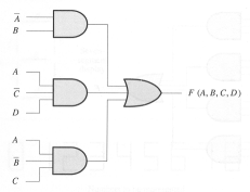
Gates and Boolean equations Show the Boolean equation for the function F described by the following circuit:

             _       _       _
F(A,B,C,D) = A*B + A*C*D + A*B*C
Discussed in section Consider the circuit shown below. Each of the control inputs, C0 through C3, must be tied to a constant, either 0 or 1.

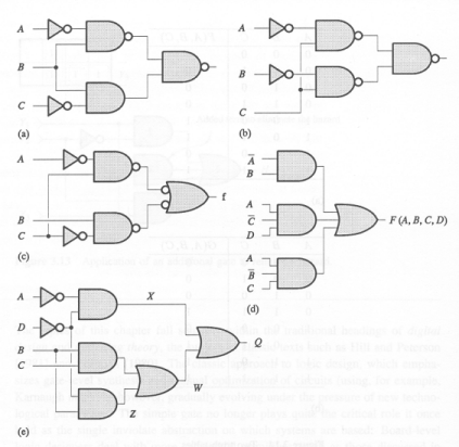
What are the values of C0 through C3 that would cause F to be the exclusive OR of A and B? We want F to be 1 when A=1 and B=0, or when A=0 and B=1. So C0 = 0, C1 = 1, C2 = 1, C3 = 0. Discussed in section Can any arbitrary Boolean function of A and B be realized through appropriate wiring of the control signals C0 through C3? Yes. This circuit implements a 4-input MUX with its two select lines connected to A and B. By choosing the appropriate values for C0 through C3 we can implement any of the 16 possible Boolean functions of A and B. Give a sum-of-products expression for each of the following circuits:

      _     _
(A) = A*B + B + C
      _     _
(B) = A*C + B*C
      _       _
(C) = A*C + B*C
      _       _       _
(D) = A*B + A*C*D + A*B*C
      _ _           _
(E) = A*D + B*C + B*D
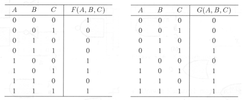
Give a canonical sum-of-products expression for the Boolean function described by each truth table below

We can construct a sum-of-products expression from a truth table by writing down a product term for each line of the table where the output is 1. Each product term contains all the input variables: directly (ie, "A") if that variable is 1 for this line of the truth table, or negated (ie, "not A") if that variable is 0 for this line of the truth table. We then OR the product terms together to get the final expression:

           _ _ _     _ _     _
F(A,B,C) = A*B*C + A*B*C + A*B*C + A*B*C
           _         _         _
G(A,B,C) = A*B*C + A*B*C + A*B*C + A*B*C
We've seen that there are a total of sixteen 2-input Boolean functions. How many 5-input Boolean functions are there? There are 225 = 232 5-input boolean functions. To see why, recall that the truth table for a 5-input function will have 32 rows, one for each possible combination of the 5 inputs. The output column for each row can be filled in with one of two choices ("0" or "1"), for a total of 232 possible ways of filling in the output column for all 32 rows.
A priority encoder has inputs that are assigned some predetermined order. The output is the binary encoding of the first "1" valued input from the ordered list, and it is zero otherwise. Discussed in section Give the truth table for a 3-input priority encoder. Assume the inputs are A, B, C with A having priority 3, B priority 2 and C priority 1:
A  B  C | P1 P0
========|=========
0  0  0 |  0  0
0  0  1 |  0  1
0  1  0 |  1  0
0  1  1 |  1  0
1  0  0 |  1  1
1  0  1 |  1  1
1  1  0 |  1  1
1  1  1 |  1  1
Discussed in section Give a sum of products realization of this priority encoder.
     _   _   _         _ _     _         _
P1 = A*B*C + A*B*C + A*B*C + A*B*C + A*B*C + A*B*C = A + B
     _ _       _ _     _         _               _
P0 = A*B*C + A*B*C + A*B*C + A*B*C + A*B*C = A + B*C
Suppose we are building circuits using only the following three components:

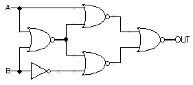
Consider the following circuit constructed from an inverter and four 2-input NOR gates:

Discussed in section What is tPD for this circuit? tPD for the circuit is the maximum cumulative propagation delay considering all paths from any input to any output. In this circuit, the longest path involves three 2-input NAND gates with a cummulative tPD = 6ns. Discussed in section What is tCD for this circuit? tCD for the circuit is the minimum cumulative contamination delay considering all paths from any input to any output. In this circuit, the shortest path involves two 2-input NAND gates with a cumulative tCD = 1ns. Discussed in section What is the output rise time for this circuit? The output rise time is determined by tr of the gate connected to OUT. In this case, it's a 2-input NAND with tr = 1.2ns. Discussed in section What is tPD of the fastest equivalent circuit (i.e., one that implements the same function) built using only the three components listed above? The most straightforward way to determine the functionality of a circuit is to build a truth table:

A  B  | OUT
======|=====
0  0  |  1
0  1  |  0
1  0  |  1
1  1  |  0
from which we can see that OUT = not B. We can implement this with a single inverter that has a tPD = 1ns.
Suppose that each component in the circuit below has a propagation delay (tpd) of 10ns, a contamination delay (tcd) of 1ns, and negligable rise and fall times. Suppose initially that all four inputs are 1 for a long time and then the input D changes to 0.

Draw a waveform plot showing how X, Y, Z, W and Q change with time after the input transition on D. First assume that the gates are not lenient. How will the waveforms change if the gates are lenient? Waveforms with non-lenient gates:

Waveforms with lenient gates:
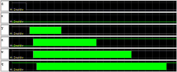
where we see that X doesn't change since the value of A is sufficient to determine the value of X. The Mysterious Circuit X Determine the function of the Circuit X, below, by writing out and examining its truth table. Give a minimal sum-of-products Boolean expression for each output.
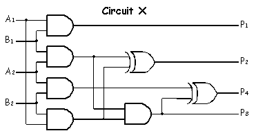
For Circuit X assume that AND gates have a propagation of 2 nS and a contamination delay of 1nS, while XOR gates have a propagation delay of 3 nS and contamination delay of 2 nS.

Compute the aggregate contamination and propagation delays for Circuit X. What is the maximum frequency that the inputs of Circuit X be changed while insuring that all outputs are stable for 5 nS? The contamination delay of the circuit is obtained from the shortest path form an input to an output. In circuit X this path start at A1 (or B1) and ends at P1, encountering only one AND gates. Thus tCD = 1ns.

The propagation delay of the circuit is obatined from the longest path from an input to an output. In circuit X this path starts at any of the inputs and ends at P4, encoutering two AND gates and one XOR gate. Thus tPD = 2ns + 2ns + 3ns = 7ns.

The answer to the next part is best understood by drawing a timing diagram:

Thus if the inputs transition no faster than every 11ns (~90 MHz), the outputs will be stable for at least 5ns. Suppose the gates below are added to Circuit X. How are the answers to part b) affected?

The shortest path from input to output now passes through three AND gates for outputs P1 and P8 and one AND gate and an XOR gate for outputs P2 and P4. Thus

tCD = min(1ns + 1ns + 1ns, 1ns + 2ns) = 3ns.

The path that creats the largest propagation delay in the circuit is still the path from any input to P4, so tPD is still 7ns.

With this new circuit the inputs can transition every 9ns and still guarantee that the outputs will be stable for 5ns.

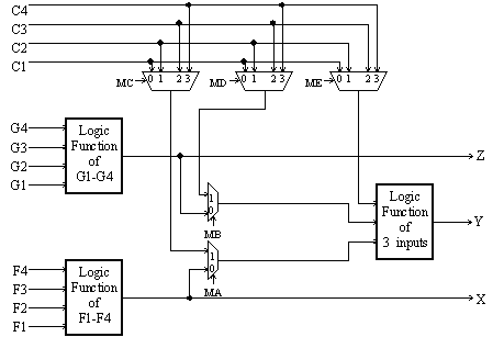
The Xilinx 4000 series field-programmable gate array (FPGA) can be programmed to emulate a circuit made up of many thousands of gates; for example, the XC4025E can emulate circuits with up to 25,000 gates. The heart of the FPGA architecture is a configurable logic block (CLB) which has a combinational logic subsection with the following circuit diagram:

There are two 4-input function generators and one 3-input function generator, each capable of implementing an arbitrary Boolean function of its inputs.

The function generators are actually small 16-by-1 and 8-by-1 memories that are used as lookup tables; when the Xilinx device is "programmed" these memories are filled with the appropriate values so that each generator produces the desired outputs. The multiplexer select signals (labeled "Mx" in the diagram) are also set by the programming process to configure the CLB. After programming, these Mx signals remain constant during CLB operation.

The following is a list of the possible configurations. For each configuration indicate how each the control signals should be programmed, which of the input lines (C1-C4, F1-F4, and G1-G4) are used, and what output lines (X, Y, or Z) the result(s) appear on. An arbitrary function F of up to four input variables, plus another arbitrary function G of up to four unrelated input variables, plus a third arbitrary function H of up to three unrelated input variables. Let X = F(F1, F2, F3, F4), Z = G(G1, G2, G3, G4), Y = H(C1, C2, C3). The necessary control signals are:

An arbitrary single function of five variables. Let Y = F(A1, A2, A3, A4, A5). This can be implemented using both 4-input logic functions, and selecting between the two outputs with the 3-input logic function.

    Z=f(A1, A2, A3, A4, 0),
    X=f(A1, A2, A3, A4, 1),
    Y= Z if A5=0, else Y=X

So Z is calculating F for the case when A5 = 0, X is calculating F for the case when A5 = 1, and Y is selecting between X and Z with a multiplexer function. A1-A4 represents F1-F4 and G1-G4 (they're connected to the same 4 inputs) and A5 represents C1. The necessary control signals are:

    MA = 0
    MB = 0
    MC = X (value doesn't matter)
    MD = X (value doesn't matter)
    ME = 0 (select C1)
An arbitrary function of four variables together with some functions of six variables. Characterize the functions of six variables that can be implemented. Let Z = G(G1, G2, G3, G4) - any function of 4 variables.

    X = F(F1, F2, F3, F4)
    Y = H(C1, C2, X) = H(C1, C2, F(F1, F2, F3, F4))

The functions of six variables which can be implemented (along with the 4-variable function) are all those functions that can be re-written as a function of 3 variables. The inputs to this function of three variables must be 2 of the original variables and some function of the remaining four variables. The necessary control signals are:

    MA = 0
    MB = 1
    MC = X (value doesn't matter)
    MD = 0 (select C1)
    ME = 1 (select C2)
Some functions of up to nine variables. Characterize the functions of up to nine variables that can be implemented. Let

    X = F(F1, F2, F3, F4)
    Z = G(G1, G2, G3, G4)
    Y = H(C1, X, Z) = H(C1, F(F1, F2, F3, F4), G(G1, G2, G3, G4))

The functions of nine variables that can be implemented are all those functions that can be re-written as a function of 3 variables. The inputs to this three-variable function will be one of the original variables, plus two separate functions of 4 variables (these two 4-variable functions will have the remaining 8 original variables as inputs).

    MA = 0
    MB = 0
    MC = X (value doesn't matter)
    MD = X (value doesn't matter)
    ME = 0 (select C1)
[Optional challenge] Can every function of six inputs be implemented? If so, explain how. If not, give a 6-input function and explain why it can't be implemented in the CLB. The functions of 6 variables which we can implement must be of the form

    Y = y(C1, C2, f(F1,F2,F3,F4))

or of the form

    Y = y(C1, f(F1, F2, F3, F4), g(G1, G2, G3, G4))

(this second function will have some overlap between C1, F1-4, and G1-4; some variables will be connected to multiple inputs) Essentially, the functions we are able to implement are only those for which we can factor a set of 4 variables out of the equation. For example, the following function cannot be implemented by the CLB:

    Y = A1A2A3A4A5 + A1A2A3A4A6 + A1A2A3A5A6 + A1A2A4A5A6
    + A1A3A4A5A6 +A2A3A4A5A6

This function cannot be broken down into either of the forms mentioned above.