In the Buba, a 5-stage pipeline without bypass logic, the result of an
instruction will not be available to be read (in the Register File
stage) until 4 clock cyles later. So for instance, if a certain
instruction writes a value to R0, that value cannot be used by the
next 3 instructions (they will all be reading the previous value of
R0). The fourth instruction (following the original instruction) is
the first that will be able to read the new value of R0. So, for
instance, consider the following code:
ADDC(R31, 10, RO)
SUBC(R0, 5, R1)
ANDC(R0, 6, R2)
ORC(R0, 7, R3)
CMPLTC(R0, 11, R4)
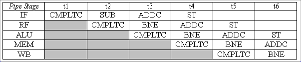
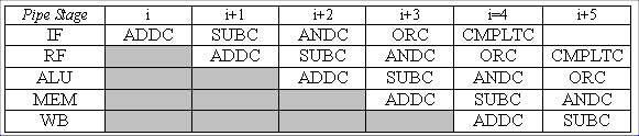 The CMPLTC will be the first instruction to fetch the new value of
R0. All the preceding instructions will be using the previous value(s)
of R0. The ADDC instruction is in the Write Back stage while ORC is in
the Register File stage-so the new R0 is not written back in time for
the ORC to read it.
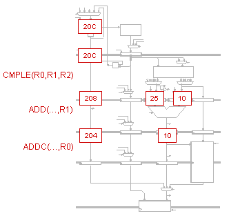
For the working Beta, S1, S2, and S3 all compute the same results.
Initially: Reg[ R1 ] = -1, Reg[ R2 ] = 1, Reg[ R3 ] = 5, Reg[ R4 ] = -1
The CMPLTC will be the first instruction to fetch the new value of
R0. All the preceding instructions will be using the previous value(s)
of R0. The ADDC instruction is in the Write Back stage while ORC is in
the Register File stage-so the new R0 is not written back in time for
the ORC to read it.
For the working Beta, S1, S2, and S3 all compute the same results.
Initially: Reg[ R1 ] = -1, Reg[ R2 ] = 1, Reg[ R3 ] = 5, Reg[ R4 ] = -1
ADD( R1, R2, R3 )         Reg[ R3 ] = Reg[ R1 ] + Reg[ R2 ] = (-1) + 1 = 0
SUB( R2, R3, R4 )         Reg[ R4 ] = Reg[ R2 ] - Reg[ R3 ] = 1 - 0 = 1
CMPLT( R3, R4, R5 )       Reg[ R5 ] = (Reg[ R3 ] < Reg[ R4 ]) = (0 < 1) = 1
so Reg[ R5 ] = 1 for all three cases.
For the Buba (italics denote cases in which the Buba is different from
a working Beta, in which the most recently calculated result is not
being used):
S1:
ADD( R1, R2, R3 )        Reg[ R3 ] = Reg[ R1 ] + Reg[ R2 ] = (-1) + 1 = 0
   new value of Reg[R3] not available yet
SUB( R2, R3, R4 )        Reg[ R4 ] = Reg[ R2 ] - Reg[ R3 ] = 1 - 5 = -4
   new values of Reg[ R3 ] and Reg[ R4 ] not available yet
CMPLT( R3, R4, R5 )      Reg[ R5 ] = (Reg[ R3 ] < Reg[ R4 ]) = (5 < -1) = 0
   Reg[ R5 ] = 0

S2:
ADD( R1, R2, R3 )        Reg[ R3 ] = Reg[ R1 ] + Reg[ R2 ] = (-1) + 1 = 0
NOP
   new value of Reg[ R3 ] not available yet
SUB( R2, R3, R4 )        Reg[ R4 ] = Reg[ R2 ] - Reg[ R3 ] = 1 - 5 = -4
NOP
   new value of Reg[ R4 ] not available yet (but Reg[ R3 ] is available)
CMPLT( R3, R4, R5 )      Reg[ R5 ] = (Reg[ R3 ] < Reg[ R4 ]) = (0 < -1) = 0
   Reg[ R5 ] = 0

S3:
ADD( R1, R2, R3 )        Reg[ R3 ] = Reg[ R1 ] + Reg[ R2 ] = (-1) + 1 = 0
NOP
   new value of Reg[ R3 ] not available yet
SUB( R2, R3, R4 )        Reg[ R4 ] = Reg[ R2 ] - Reg[ R3 ] = 1 - 5 = -4
   new values of Reg[ R3 ] and Reg[ R4 ] not available yet
CMPLT( R3, R4, R5 )       Reg[ R5 ] = (Reg[ R3 ] < Reg[ R4 ]) = (5 < -1) = 0
   Reg[ R5 ] = 0
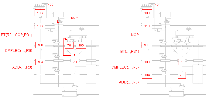
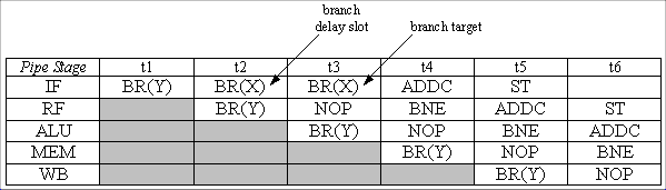
 In a 5-stage pipelined Beta, when does the hardware use its
ability to insert NOP into the instruction stream at the IF stage
(using the MUX controlled by AnnulIF)?
In a 5-stage pipelined Beta, when does the hardware use its
ability to insert NOP into the instruction stream at the IF stage
(using the MUX controlled by AnnulIF)?
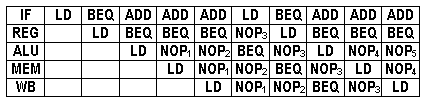


 P-R-U reasons that instructions that leave out the MEM stage can
complete a cycle earlier and thus most programs will run 20% faster!
In your answers below assume that both the original and the P-R-U
pipelined implementations are fully bypassed.
P-R-U reasons that instructions that leave out the MEM stage can
complete a cycle earlier and thus most programs will run 20% faster!
In your answers below assume that both the original and the P-R-U
pipelined implementations are fully bypassed.
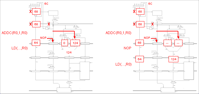
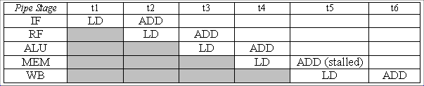 The stall occurs when the ADD and the LD attempt to use the WB stage
at the same time, forcing the ADD instruction to remain in a wait
stage during t5.
The stall occurs when the ADD and the LD attempt to use the WB stage
at the same time, forcing the ADD instruction to remain in a wait
stage during t5.

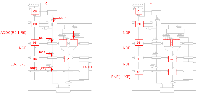
 The interrupt causes the address 0x123C to be stored in XP. When
the interrupt handler is done it should return to the SUB instruction
at 0x1238. If it would return to the address in the XP, then the SUB
instruction would never get executed, because it was not executed
before the interrupt handler.
The interrupt causes the address 0x123C to be stored in XP. When
the interrupt handler is done it should return to the SUB instruction
at 0x1238. If it would return to the address in the XP, then the SUB
instruction would never get executed, because it was not executed
before the interrupt handler.

 After the interrupt handler is finished, it will return to the
CMPLTC instruction. That clearly is not the correct behavior because
we want the branch to be taken and CMPLTC to be annulled.
After the interrupt handler is finished, it will return to the
CMPLTC instruction. That clearly is not the correct behavior because
we want the branch to be taken and CMPLTC to be annulled.
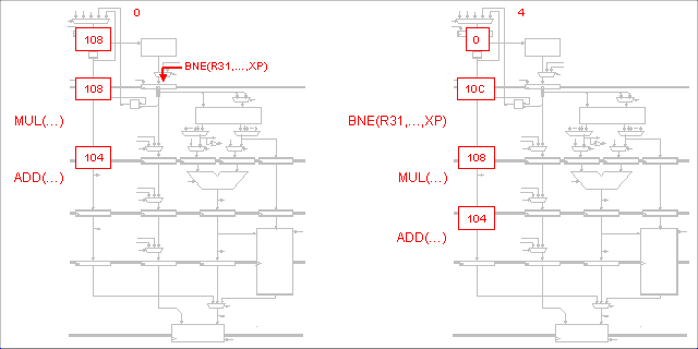
 The address stored in XP is the instruction following the BR(X), so
when returning from the interrupt handler, then the XP is adjusted so
it has the address of the BR(X). A similar argument could be made if
the interrupt arrives while annulling the branch delay slot of the
BR(X) instruction.
The address stored in XP is the instruction following the BR(X), so
when returning from the interrupt handler, then the XP is adjusted so
it has the address of the BR(X). A similar argument could be made if
the interrupt arrives while annulling the branch delay slot of the
BR(X) instruction.