Which of the following cannot be made to function with perfect
reliability, assuming reliable components and connections.
Explain your reasoning. Some of the specifications refer
to "bounded time" which means there is a specified time interval,
measured from the most recent input transition, after which the
output is stable and valid.
 A circuit that in unbounded time indicates which of two game show
contestants pressed their button first.
It is possible to build this unbounded-time arbiter. It may
take an arbitrary period, after which it will produce (1) a
decision and (2) a signal that indicates that its made a
decision.
A circuit that in bounded time indicates which of two game show
contestants pressed their button first.
This is a restatement of the "bounded time arbiter problem",
known to be unsolvable in theory. In practice we can build a circuit
to solve this problem where the probability of failure is related
to tPD. For "large" tPD (eg, 10's of nanoseconds in today's
technologies) the probability of failure can be made very
small (eg, 1 failure in billions of years).
A circuit that determines if button A was pressed before a specified
deadline. Assume the circuit has an accurate internal signal that
transitions from 0 to 1 when the deadline is reached. The output
should be 1 if the button was pressed on or before the deadline, 0 if
pressed after the deadline. The output should be valid and stable
within a specified tPD of the A input transition.
This is another restatement of the "bounded time arbiter problem",
known to be unsolvable in theory. Of course, given sufficiently long
time bounds, we can engineer practical approximate solutions (see the
answer to the previous question).
A circuit that in bounded time indicates which of two game show
contestants pressed their button first if the presses were more than
0.1 second apart, otherwise the circuit lights up a "TIE" light.
This circuit will suffer metastability problems because the decision
as to whether the presses were 0.1 seconds apart is subject to
metastability problems.
A circuit that in bounded time indicates that at least one button has
been pressed by some contestant.
An OR gate will do the job.
A circuit that in bounded time indicates that exactly one of the
contestants has pressed their button. You can assume there are only
two contestants.
An XOR gate will meet the spec.
A circuit that has two parts: (a) a subcircuit that indicates which of
two game show contestants pressed their button first, and (b) a
subcircuit that in bounded time lights a "TIE" light if the (a)
subcircuit hasn't produced an answer after 1 second. The "TIE" light
should stay lit even if (a) makes a decision at some later point.
Both subcircuits will suffer metastability problems. (a) is asking
for an arbiter (see part B above) and (b) has the same difficulties as
outlined for part C above.
A circuit that converts button presses from two contestants into the
following two-bit output encoding. The circuit has two inputs, A and
B, one for each contestant. A contestant's input transitions from 0
to 1 when she presses her button.
A circuit that in unbounded time indicates which of two game show
contestants pressed their button first.
It is possible to build this unbounded-time arbiter. It may
take an arbitrary period, after which it will produce (1) a
decision and (2) a signal that indicates that its made a
decision.
A circuit that in bounded time indicates which of two game show
contestants pressed their button first.
This is a restatement of the "bounded time arbiter problem",
known to be unsolvable in theory. In practice we can build a circuit
to solve this problem where the probability of failure is related
to tPD. For "large" tPD (eg, 10's of nanoseconds in today's
technologies) the probability of failure can be made very
small (eg, 1 failure in billions of years).
A circuit that determines if button A was pressed before a specified
deadline. Assume the circuit has an accurate internal signal that
transitions from 0 to 1 when the deadline is reached. The output
should be 1 if the button was pressed on or before the deadline, 0 if
pressed after the deadline. The output should be valid and stable
within a specified tPD of the A input transition.
This is another restatement of the "bounded time arbiter problem",
known to be unsolvable in theory. Of course, given sufficiently long
time bounds, we can engineer practical approximate solutions (see the
answer to the previous question).
A circuit that in bounded time indicates which of two game show
contestants pressed their button first if the presses were more than
0.1 second apart, otherwise the circuit lights up a "TIE" light.
This circuit will suffer metastability problems because the decision
as to whether the presses were 0.1 seconds apart is subject to
metastability problems.
A circuit that in bounded time indicates that at least one button has
been pressed by some contestant.
An OR gate will do the job.
A circuit that in bounded time indicates that exactly one of the
contestants has pressed their button. You can assume there are only
two contestants.
An XOR gate will meet the spec.
A circuit that has two parts: (a) a subcircuit that indicates which of
two game show contestants pressed their button first, and (b) a
subcircuit that in bounded time lights a "TIE" light if the (a)
subcircuit hasn't produced an answer after 1 second. The "TIE" light
should stay lit even if (a) makes a decision at some later point.
Both subcircuits will suffer metastability problems. (a) is asking
for an arbiter (see part B above) and (b) has the same difficulties as
outlined for part C above.
A circuit that converts button presses from two contestants into the
following two-bit output encoding. The circuit has two inputs, A and
B, one for each contestant. A contestant's input transitions from 0
to 1 when she presses her button.
00 if neither contestant is pressing their button
01 if contestant A is pressing her button
10 if contestant B is pressing her button
11 if both contestants are pressing their buttons
The output should be valid and stable within a specified tPD of
the most recent input transition.
Easy! The low-order bit of the encoding is the signal from A, the
high-order bit is the signal from B. Nothing to go metastable here.
A judge is routinely given 60 seconds to make yes-or-no decisions.
Which of the following techniques allows him to do it with perfect
reliability, in light of the unrealizability of a perfect bounded-time
arbiter?
He can do it reliably simply by flipping a coin.
In theory the coin flip has its own metastability problem: the coin
may balance on its edge and hence may not reliably produce an answer in the time
required. Since the judge is depending on the coin, he may also not
produce an answer in the time required.
In general the mapping of any continuous input variable (eg, the position
of the coin) into a discrete output value (eg, "yes" or "no") is subject to
metastability problems if all input values have to be mapped in
bounded time to valid output values.
He can do it reliably by asking his clerk and responding "yes" unless
his clerk has answer in 55 seconds.
The decision as to whether the clerk has answered in 55 seconds is
subject to metastability problems, hence the judge may not respond
reliably.
He can do it realiably by always answering "no", independently of
the question.
It's true the judge will always respond reliably. Ignoring the
input is a valid (if not very satisfying) technique for solving the
metastability problem.
Cambridge Logic and Magic, Inc is a new startup founded by a group of
ex-MIT students who dropped out of 6.004 just before Lecture 8. They
are trying to develop a reliable, bounded-time arbiter that behaves as
follows:
Two combinational inputs, A and B, each have a single 0-to-1
transition. The arbiter has a single output, which may be safely
sampled one microsecond following the transition on the A input, at
which point it is guaranteed (with 100% reliability) to have a valid
logic level. If the A transition precedes the B transition by more
than 100ns, the output is to be 0 when sampled; if the B transition
precedes A by more than 100ns, the output is to be 1 when sampled. If
the transitions are within 100ns of each other, either a 1 or a 0 may
be present. In all cases, the output is stable and valid for a 10ns
interval surrounding the time at which it is to be sampled.
The four CLMI founders each have a proposed design for such an
arbiter. Your job is to identify the problem in each design, citing a
specific scenario in which it fails to meet its spec. [If you're
unable to convince yourself that any scheme doesn't work, perhaps you
should consider dropping out and starting a company!]
Assume in the following designs that (1) All registers start in the 0
state; (2) that transitions on each of the input signals are
instantaneous and surrounded by long setup and hold times; and (3)
that component timings are short compared to the one microsecond
delay.
The first scheme involves a D register and a lenient MUX. It's
proponent argues that it can't go metastable, since the dynamic
discipline is always obeyed on the register inputs.
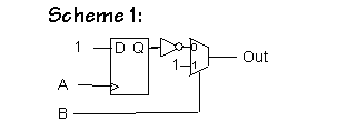 It's true that this circuit has no metastability problems, but it
gets the wrong answer.
Suppose the A transition happens more than 100ns
before the B transition but the output is sampled after the B
transition has arrived and propagated through the MUX. Under this
situation the output will be a 1 when it is supposed to be a 0.
The second scheme involves a 50ns delay and a lenient OR gate. If the
output of the register is metastable, the inventor argues, the gate's
output will be forced to a valid level by the delayed copy of A. The
delay is 50 ns.
It's true that this circuit has no metastability problems, but it
gets the wrong answer.
Suppose the A transition happens more than 100ns
before the B transition but the output is sampled after the B
transition has arrived and propagated through the MUX. Under this
situation the output will be a 1 when it is supposed to be a 0.
The second scheme involves a 50ns delay and a lenient OR gate. If the
output of the register is metastable, the inventor argues, the gate's
output will be forced to a valid level by the delayed copy of A. The
delay is 50 ns.
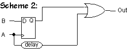 This circuit also has no metastability problems, but it too
gets the wrong answer.
Suppose the A transition happens more than 100ns before
the B transition. Since the output is sampled one microsecond after the
A transition happens, that transition will have enough time to propagate through the
delay and through the OR gate. Since the OR gate is lenient it will output
a 1 regardless of what the input from the register is (even if the register
is metastable). Thus, regardless of which signal arrives first, the output
will always be a 1. But the output should be 0 when A happens at least 100ns
before B.
The third scheme involves a pair of D registers sharing the B input.
The delay is 50 ns, a time chosen to ensure that if setup/hold times
are violated for either of the registers the other will see valid
input timing. The OR gate is lenient.
This circuit also has no metastability problems, but it too
gets the wrong answer.
Suppose the A transition happens more than 100ns before
the B transition. Since the output is sampled one microsecond after the
A transition happens, that transition will have enough time to propagate through the
delay and through the OR gate. Since the OR gate is lenient it will output
a 1 regardless of what the input from the register is (even if the register
is metastable). Thus, regardless of which signal arrives first, the output
will always be a 1. But the output should be 0 when A happens at least 100ns
before B.
The third scheme involves a pair of D registers sharing the B input.
The delay is 50 ns, a time chosen to ensure that if setup/hold times
are violated for either of the registers the other will see valid
input timing. The OR gate is lenient.
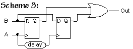 This scheme fails when the B transition happens 50ns after the A
transition. In this situation the first register will output a 0 since
the rising edge of the A signal arrived before B transitioned from 0
to 1. However, in the second register, the D input arrives at the same
time as the clock. Thus the register may become metastable and generate
an invalid output. So the OR gate receives a 0 input from the
first register and a potentially invalid input from the second register.
Thus the OR gate may also generatate an invalid output.
The fourth scheme involves a pair of D register and a delay similar
to Scheme 3, but uses a MUX to select the output from a non-metastable
flipflop:
This scheme fails when the B transition happens 50ns after the A
transition. In this situation the first register will output a 0 since
the rising edge of the A signal arrived before B transitioned from 0
to 1. However, in the second register, the D input arrives at the same
time as the clock. Thus the register may become metastable and generate
an invalid output. So the OR gate receives a 0 input from the
first register and a potentially invalid input from the second register.
Thus the OR gate may also generatate an invalid output.
The fourth scheme involves a pair of D register and a delay similar
to Scheme 3, but uses a MUX to select the output from a non-metastable
flipflop:
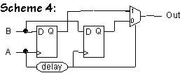 Since the output is sampled 1 microsecond after the A transition
happens, the transition as enough time to propagate through the
delay, into the MUX where it switches MUX to output the result
of the first register. Thus the circuit effectively consists of
the first register. If the A transitions happens at the same time
as the B transition, then first register may be metastable and
may generate an invalid output, causing the MUX to generate an
invalid output.
Ben Bitdiddle has been hired as a consultant by Two Bit Electronics, a
firm specializing in communications channels that are two bits wide.
TBE has discovered that its latest product has been failing now and
then at various customer sites and is worried that the design may have
a problem with metastability.
Ben starts by checking the schematics for one bit of the transmission
channel:
Since the output is sampled 1 microsecond after the A transition
happens, the transition as enough time to propagate through the
delay, into the MUX where it switches MUX to output the result
of the first register. Thus the circuit effectively consists of
the first register. If the A transitions happens at the same time
as the B transition, then first register may be metastable and
may generate an invalid output, causing the MUX to generate an
invalid output.
Ben Bitdiddle has been hired as a consultant by Two Bit Electronics, a
firm specializing in communications channels that are two bits wide.
TBE has discovered that its latest product has been failing now and
then at various customer sites and is worried that the design may have
a problem with metastability.
Ben starts by checking the schematics for one bit of the transmission
channel:
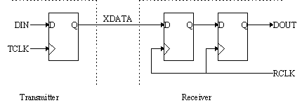 A TBE engineer explains that although TCLK and RCLK have the same
frequency, their phases may differ. Ben notes with approval the 2
D-registers in the receiver, which are configured as a pulse
synchronizer, a circuit intended to ensure that the probability of
DOUT entering the metastable state is very small. Briefly explain how
the pulse synchronizer accomplishes this goal. Hint: Because the
input to the receiver is asynchronous with RCLK, the left-most
register in the receiver can enter a metastable state. But the
probability that the input to the right-most register in the receiver
does not meet that register's setup time can be made as small as
desired by increasing the period of RCLK. Why?
Whenever we create a circuit that has an input generated by a system
running with a different clock (or no clock at all), we run the risk
of entering a metastable state in our registers that use this
input. This can happen since the asynchronous input could be
transitioning during the period of time before and after the rising
clock edge that a register requires the input to be stable. However,
the longer a signal stays in a positive-feedback storage element (like
those in a register), the more likely it is to leave the metastable
state and yield a valid output level. By chaining registers together,
we increase the amount of time during which the signal stays in a
positive-feedback loop before we use its value in our logic.
The engineer now shows Ben the schematic for a test jig that he says
illustrates the problem that's been discovered. The test jig consists
of two one-bit channels running in parallel with the two DIN inputs of
the transmitter connected to a single data stream. The DOUT outputs
of the two receivers are connected to an XOR gate that, in theory,
should always produce a "0" since both receivers are getting the same
data stream. In order to filter out any glitches in the XOR output
introduced by small differences in tPD of the output registers of the
two receivers another register has been added to the output of the XOR
gate:
A TBE engineer explains that although TCLK and RCLK have the same
frequency, their phases may differ. Ben notes with approval the 2
D-registers in the receiver, which are configured as a pulse
synchronizer, a circuit intended to ensure that the probability of
DOUT entering the metastable state is very small. Briefly explain how
the pulse synchronizer accomplishes this goal. Hint: Because the
input to the receiver is asynchronous with RCLK, the left-most
register in the receiver can enter a metastable state. But the
probability that the input to the right-most register in the receiver
does not meet that register's setup time can be made as small as
desired by increasing the period of RCLK. Why?
Whenever we create a circuit that has an input generated by a system
running with a different clock (or no clock at all), we run the risk
of entering a metastable state in our registers that use this
input. This can happen since the asynchronous input could be
transitioning during the period of time before and after the rising
clock edge that a register requires the input to be stable. However,
the longer a signal stays in a positive-feedback storage element (like
those in a register), the more likely it is to leave the metastable
state and yield a valid output level. By chaining registers together,
we increase the amount of time during which the signal stays in a
positive-feedback loop before we use its value in our logic.
The engineer now shows Ben the schematic for a test jig that he says
illustrates the problem that's been discovered. The test jig consists
of two one-bit channels running in parallel with the two DIN inputs of
the transmitter connected to a single data stream. The DOUT outputs
of the two receivers are connected to an XOR gate that, in theory,
should always produce a "0" since both receivers are getting the same
data stream. In order to filter out any glitches in the XOR output
introduced by small differences in tPD of the output registers of the
two receivers another register has been added to the output of the XOR
gate:
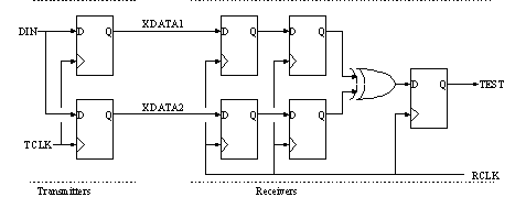 Every once in a while TEST is observed to be "1" for one period of
RCLK. Give a brief explanation of why this happens. You can assume
that DIN is meeting the setup time of the transmitter registers and
that the value for DIN changes much less frequently than TCLK/RCLK.
Hint: it has nothing to do with the register that was added to
deglitch the TEST output. Think about what's happening in the two
pulse synchronizers and why they might generate different outputs for
a single clock cycle.
A first-look at the test jig seems to imply that DOUT should always be
0, since XDATA1=XDATA2. However, when a register enters a metastable
state, we don't know which value the output will eventually
reach. Thus, if one or both of the registers enters a metastable
state, its output could be either 0 or 1. Thus, the output of the two
registers could be different causing the XOR gate to generate a 1.
TBE now realizes that their plan to send two bits at a time by using
two independent synchronizers won't work. "Okay," they say, "we'll
just transmit one bit at a time, use a single synchronizer and crank
up the clock frequency." Ben observes that this circuit still won't
result in completely accurate communication, i.e., the waveform
produced by the receiver on DOUT still won't be the same as the
waveform produced by the transmitter on XDATA. Give a brief
explanation of why Ben is right.
Pulse synchronizers can be used to solve metastability problems
arising from asynchronous inputs but the synchronization process
introduces changes in the timing of the data waveform. All
transitions in the bit stream output by the synchronizer will happen
on the rising edge of the receiver clock, and hence the timing between
transitions will be some multiple of the receiver clock period. If
there was information carried by the timing of transitions in the
transmitted bit stream, it's lost (or at least garbled) by the
synchronizers.
Ben explains that communications between asynchronous systems is a
tricky business! If the input stream isn't too fast compared to the
receive clock, a pulse synchronizer will reliably reproduce any
transitions in the input waveform, although the exact timing between
the transitions in the output waveform will not the same as in the
incoming waveform.
[Hard] Can you think of a way to encode a bit stream using
transitions rather than levels to convey the information? Describe
your encoding scheme and the signals that would be output by your
receiver.
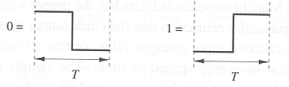
Manchester encoding can be used to transmit a stream of bits
over a single data wire, with no auxiliary clock information. Each
bit is represented by one of the following patterns, where T is the
period of the clock used to encode the signal. Note that a
Manchester-encoded signal always changes value in the middle of each
bit cell.
Every once in a while TEST is observed to be "1" for one period of
RCLK. Give a brief explanation of why this happens. You can assume
that DIN is meeting the setup time of the transmitter registers and
that the value for DIN changes much less frequently than TCLK/RCLK.
Hint: it has nothing to do with the register that was added to
deglitch the TEST output. Think about what's happening in the two
pulse synchronizers and why they might generate different outputs for
a single clock cycle.
A first-look at the test jig seems to imply that DOUT should always be
0, since XDATA1=XDATA2. However, when a register enters a metastable
state, we don't know which value the output will eventually
reach. Thus, if one or both of the registers enters a metastable
state, its output could be either 0 or 1. Thus, the output of the two
registers could be different causing the XOR gate to generate a 1.
TBE now realizes that their plan to send two bits at a time by using
two independent synchronizers won't work. "Okay," they say, "we'll
just transmit one bit at a time, use a single synchronizer and crank
up the clock frequency." Ben observes that this circuit still won't
result in completely accurate communication, i.e., the waveform
produced by the receiver on DOUT still won't be the same as the
waveform produced by the transmitter on XDATA. Give a brief
explanation of why Ben is right.
Pulse synchronizers can be used to solve metastability problems
arising from asynchronous inputs but the synchronization process
introduces changes in the timing of the data waveform. All
transitions in the bit stream output by the synchronizer will happen
on the rising edge of the receiver clock, and hence the timing between
transitions will be some multiple of the receiver clock period. If
there was information carried by the timing of transitions in the
transmitted bit stream, it's lost (or at least garbled) by the
synchronizers.
Ben explains that communications between asynchronous systems is a
tricky business! If the input stream isn't too fast compared to the
receive clock, a pulse synchronizer will reliably reproduce any
transitions in the input waveform, although the exact timing between
the transitions in the output waveform will not the same as in the
incoming waveform.
[Hard] Can you think of a way to encode a bit stream using
transitions rather than levels to convey the information? Describe
your encoding scheme and the signals that would be output by your
receiver.
Manchester encoding can be used to transmit a stream of bits
over a single data wire, with no auxiliary clock information. Each
bit is represented by one of the following patterns, where T is the
period of the clock used to encode the signal. Note that a
Manchester-encoded signal always changes value in the middle of each
bit cell.
 A block diagram of a Manchester decoder is shown below.
The decoder is a clocked sequential machine whose state memory consists
of just two edge-triggered D flip-flops.
A block diagram of a Manchester decoder is shown below.
The decoder is a clocked sequential machine whose state memory consists
of just two edge-triggered D flip-flops.
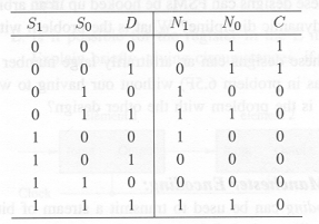
 The combinational portion of the decoder has as inputs the
Manchester-encoded signal and the current state of the two flip-flops.
The combinational logic outputs the next state N1 and N0 for the
two flip-flops and the clock signal C generated for the stream of
serial data. The truth table of the combinational logic is as
follows:
The combinational portion of the decoder has as inputs the
Manchester-encoded signal and the current state of the two flip-flops.
The combinational logic outputs the next state N1 and N0 for the
two flip-flops and the clock signal C generated for the stream of
serial data. The truth table of the combinational logic is as
follows:
 Note that the serial data out from the decoder is just a copy of
the Manchester-encoded data in. Thus the decoder must place positive
transitions in its clock output C timed to correspond to the correct
logic values already present in the Manchester-encoded stream.
The positive-going edge of each clock pulse must occur while the
Manchester-encoded data has the proper value for the serial output;
but there is no particular restriction that the clock output must
return to zero before the Manchester-encoded input changes value, or
that all output clock pulses be of the same duration or evenly spaced
in time. The sample timing diagram below shows an original stream of
serial input data and its clock, the result of Manchester-encoding
that stream, and a clock output waveform that meets the conditions
stated. (This is not intended to imply that the specific "clock
out" signal shown would actually be generated by the above circuit.)
Note that the serial data out from the decoder is just a copy of
the Manchester-encoded data in. Thus the decoder must place positive
transitions in its clock output C timed to correspond to the correct
logic values already present in the Manchester-encoded stream.
The positive-going edge of each clock pulse must occur while the
Manchester-encoded data has the proper value for the serial output;
but there is no particular restriction that the clock output must
return to zero before the Manchester-encoded input changes value, or
that all output clock pulses be of the same duration or evenly spaced
in time. The sample timing diagram below shows an original stream of
serial input data and its clock, the result of Manchester-encoding
that stream, and a clock output waveform that meets the conditions
stated. (This is not intended to imply that the specific "clock
out" signal shown would actually be generated by the above circuit.)
 The period of the "decoder clock" that drives the D flip-flops
need not be T; in general, it will be faster.
The period of the "decoder clock" that drives the D flip-flops
need not be T; in general, it will be faster.