6.111 Lab #2 Part A

Goal: implement simple circuits in Verilog and run ModelSim from command line and within ISE; download and run a sample circuit on the labkit.

Useful links

Exercise 1: Writing Verilog code

In this exercise you'll design a Verilog module that implements a 74LS163. Here are the steps:

  1. Log into one of the Athena workstations in the Digital Lab. Your username and password are your standard Athena user name and password.

    Type: tcsh
    This will ensure that the shell program you're running is cshell, which we know to have working scripts for.

    Type: add 6.111
    This will add the 6.111 locker, allowing you to access various files important for 6.111.

    Type: source /mit/6.111/tools.tcsh
    This will set up the 6.111 tools (Modelsim, Xilinx ISE and Impact).

    To run Modelsim type: vsim & (the '&' allows you to keep typing in the terminal)
    To run Xilinx ISE type: ise &
    To run Xilinx Impact type: impact &

    You can setup your environment permanently and avoid adding the locker and set up command each time you login by customizing your configuration file. First determine your shell by

    Type: ps
    Look at what is listed under the CMD column. It should be either tcsh or bash (the name of your shell program). Most accounts created after 2009 use bash.

    If you have tcsh, add the following to ~/.cshrc.mine

         add 6.111
         source /mit/6.111/tools.tcsh
    
    
    If you have bash, add the the following to ~/.bashrc.mine
         add 6.111 
         alias ise="tcsh -c 'source /mit/6.111/tools.tcsh;ise'" 
         alias vsim="tcsh -c 'source /mit/6.111/tools.tcsh;vsim'" 
         alias impact="tcsh -c 'source /mit/6.111/tools.tcsh;impact'" 
    

  2. Download lab2_1.v by right-clicking on the link and select "Save As" (or "Save Link As"), and specify a destination. It is good to be organized and put all your labs in separate folders - e.g. 6.111work/Labs/Lab2/sources/lab2_1.v.

The steps below describe how to use our Verilog simulator Modelsim as a standalone application. One can also run the simulator from the Xilinx ISE toolkit -- see the labkit documentation Simulating with Modelsim for details on how to do this. Feel free to use either approach for this part of the lab.

  1. Start Modelsim (either by typing "vsim &" or from Xilinx ISE)

  2. At the bottom of the Modelsim window there's a frame labeled "Transcript" where you can type in commands and see various messages from the simulator. Type in "cd LabFolderPath" to change to the folder where you want to run your lab, e.g. " cd 6.111work/Lab2".

  3. Type "vlib work" to set up the simulator's working library

  4. Type "vlog sources/lab2_1.v" to compile the verilog file you downloaded above. Output from the compiler is displayed in the transcript window.

  5. Type "vsim test" to start simulating the test module found in lab2_1.v.

  6. Type "run 2000ns" to run the simulation for 2000ns. You should see the following printout in the Transcript window
         # Starting test of LS163...
         # clear was asserted low, but counter didn't clear
         # out = xxxx, expected 0000
         # Break at lab2_1.v line 48
    

    These messages were generated by code inside the test module as it runs through various tests of the LS163 module. The LS163 module supplied in lab2_1.v is empty which is why the test failed. Your job is to fill in the body for the LS163 module, implementing the correct functionality. Refer to the 74LS163 datasheet to see what functionality your code needs to implement. Verilog hint: the concatenation operators {} will handle arithemtic operations correctly, eg: {qd,qc,qb,qa} + 1;

    You can use the editor of your choice to edit lab2_1.v appropriately. Modelsim has a simple built-in editor which should be displaying lab2_1.v after you completed step 8. To use the built-in editor, click on the the tool bar option "Source" and uncheck the "Read Only" line. As you edit lab2_1.v, repeat steps 6 through 8 above to test your code. When you're successful you'll see

         # Starting test of LS163...
         # Finished test of LS163...
    

  7. When your code passes the tests, have a staff member check you off. (0.9 point) Please make sure that you understand the test-jig in lab2_1.v. The staff will ask you to explain some parts of it in addition to seeing it work in Modelsim as we will be writing a lot of test-jigs for labs and project this term and good test-jig writing skills will save you a ton of time.

  8. After checkoff, please upload your Verilog file using the "Submit Verilog" page on the course website. We'll review your code and post some comments to help you improve your Verilog style. We'll be looking for proper use of comments and formatting to make your code easy to understand.

Exercise 1 (b): Modelsim - Behavior simulation, waveform display

In this exercise you'll use the ls163 code and verify operation through behavior simulation with Modelsim within ISE.

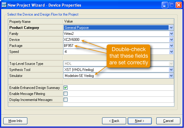
  1. Start ISE from the terminal window and create a new project (File, New Project) named lab2 in an appropriate directory on your account. Select the appropriate device properties.

  2. In the pop up window "New Source" select the source type "Verilog Module" and name it "ls163_lab2.v". From the pop up menu create the following input ports: clk,ent,enp,load,clear,a,b,c,d and output ports: qa,qb,qc,qd, rco. Click "Next" then "Finish" A skelton Verilog module has been created.

    Variables in Verilog that are set inside an "always" block (qa,qb,qc,qd) block must be declared as "reg" so insert "reg" after "output" for qa,qb,qc,qd.

  3. Open "ls163_lab2" and insert your ls163 Verilog from the previous exercise. You have now created your first Verilog module.

  4. To create a behavior testbench (Verilog Test Fixture) for your Verilog, right click on your Verilog file "ls163_lab2", click on "New Source" and select source type "Verilog Test Fixture". Name the source ls163_tb, associate the test bench with "ls163_lab2" and click finish. ISE will generate a basic testbench which instantiates the ls163 module (the unit-under-test, or UUT) and declares wire and reg signals for all of its ports. The testbench will also include the an initial block, which initializes all of the inputs to the UUT. You can extend this block to generate whatever stimulus you wish to apply to the UUT.

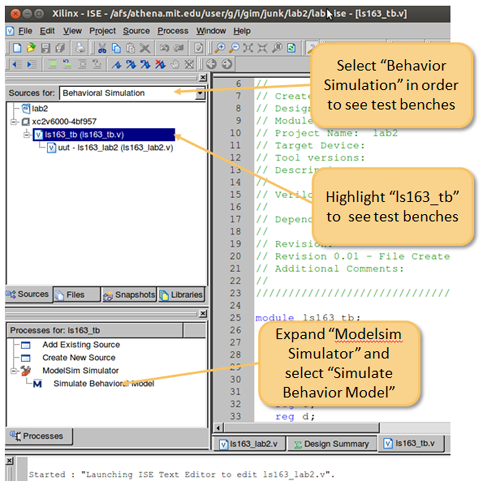
  5. In the upper left of the project navigator, under "Sources for:", select "Behavior Simulation".

    Click on the test bench "ls163_tb". To create a 10ns clock, find the line "initial begin" in your test bench and insert

    	always #5 clk = !clk;   // change state every 5ns
    before the line "initial begin". To initialize the counter to the value nine and begin counting, copy and paste the following lines your test bench "ls163_tb" after the line "// Add stimulus here"

    	//////////////////////////////////////////////
    	//
    	clear = 1; 
    	load = 0;     // note load is active low 
    	a = 1;        // now load 8'b1001 to counter
    	b = 0;       
    	c = 0; 
    	d = 1; 
    	ent = 1;      // enp = ent = 1 to count
    	enp = 1; 
    	#20;          // wait for 20ns
    	load = 1;
    	//
    	/////////////////////////////////////////////
    

    Save the changes.

  6. Running ModelSim - In the "Process for" window, expand "ModelSim Simulator". You should have the following:

    Double click on "Simulate Behavior Model". Modelsim and a Waveform window will pop up. With the mouse in the waveform window right click "Zoom Full" to view the full simulation. Simulating with Modelsim contains examples of complex test benches. You should see the counter cycle from 9-15 with RCO high on a count of 15.

  7. For checkoff, show the waveform window to the staff. (1.0 point) Note: While compiling and running Verilog is not time consuming, it is fair more efficient run simulation - especially when complex Verilog modules can take 20-60 minutes to compile.

Exercise 2: Compiling and running Verilog on the labkit

In this exercise you'll design a Verilog module that reads a 4-bit value from labkit's switches and displays the appropriate hex digit on a 7-segment display.

  1. To learn more about the Xilinx FPGA tools please read the Getting Started section of the Labkit documentation. You'll follow the steps outlined there whenever creating a new project for the labkit.

  2. Download labkit.v and labkit.ucf by right-clicking on the links and selecting "Save As" (or "Save Link As"), specify the desired folder as the destination. Note that the browser may save your downloads with a ".txt" extension -- you'll have to rename the files to have ".v" and ".ucf" extensions in order for the Xilinx tools to recognize them correctly.

    The labkit module (defined in labkit.v) has port declarations for all the labkit peripherals as well as supplying default values for all the output ports. This is the top-level module for all labkit projects -- you should make a copy of it using a meaningful file name (eg, lab2_2.v) and modify the copy to implement the circuitry for your project. labkit.ucf (which you'll never need to modify) specifies which FPGA pin is connected to which named port in labkit.v.

  3. Start the Xilinx ISE tool and create a new project following the steps outlined in the Getting Started document. The Xilinx tools create a very large number of files, so to keep things neat and tidy I recommend keeping your .v files separate from the project directory. For example, if you keep your .v files in Lab2/sources, specify Lab2/ as the location for your project directories, and when you supply a name for the project (eg, lab2_2) a directory of that name will be created in Lab2/ and used to store all the Xilinx-created files. When you add verilog source files to the project, add them from the sources/ folder.

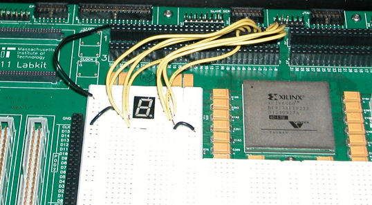
  4. We'll be using the 7-segment display from your kit of parts (this is the display you used in Exercise 6 of Lab 1), this time wired to the FPGA via the labkit's breadboard (see photo below). Wire up the display connecting its ground pins to the appropriate columns of the breadboard, and the signal pins to the User 1 connector at the top of the labkit (I used pins 0 through 7).

  5. Add Verilog code to the labkit module using four of the labkit's slide switches to specify which hex digit to display on a 7-segment display. The switch port of the labkit module is an 8-bit value reflecting the current settings of the labkit's slide switches. Use switch[3:0] as the 4-bit hex digit to be displayed. Here's the appropriate pattern of segments for each digit:

    Compute the appropriate value for each of segment control signals and drive them onto the appropriate FPGA output pins (I used user1[7:0]). (There are two rows of pins. Be sure to use the signal pins and not the grounds.) Note that you'll have to modify or comment-out the existing line in the code that sets a default value for the output pins you're using.

    Synthesize and implement your design. Generate a programming file and configure the FPGA. When your circuit is working, you should be able to display 0-f on the 7-segment display using the switches.

    Unless you following the instructions exactly, you synthesis will fail - labkit.ucf file includes constraints for all of the input and output ports defined in labkit.v. Most designs, however, will not use all of these signals, in which case the synthesis engine will optimize the unused signals out of the design. The location constraints in labkit.ucf for these unused signals will then generate errors. It is therefore necessary to tell ISE not to generate an error if it encounters a pin constraint for a (now) nonexistent signal. To do this, right-click on the "Implement Design" item in the process pane, and select "Properties...". Check the box to "allow unmatched LOC constraints" in the "Translate Properties" form.

    Add Verilog to your module by replacing 4 slide switches with the output of a 4 bit counter. Increment the count on every rising edge of button_enter.

    	//////////////////////////////////////////////
    	//
            always @(posedge button_enter)
            counter<=counter+1;
    	//
            // using the edge of an external input as a 
            // clock is poor design practice!
    	/////////////////////////////////////////////
    
    Because of switch bounce, the counter may increment by more than one. Switch bounce typically disappears after 10-20 ms. One approach to debouncing is to sample the input. The input is considered valid only if the value is the same for some period of time. Add Verilog to debounce the switch input so that each press of button_enter increments the count by one. For debouncer, a signal is considered to be clean if the value remains the same for 10msec. With a 27mhz clock, that's 270,000-1 clock cycles. Step 1: At each clock pulse, store the new input into a reg Step 2: if the new input is the same as the previous input, increment a counter. If not it must be switch bounce so set the counter to zero. When the counter reaches 270,000-1, you have a debounced input. Here's a skelton of the debounce Verilog:

    	//////////////////////////////////////////////
    	//
            module debounce(
                input clk,       // check the name of your clock
                input reset,     // system reset
                input bouncey_input,
                output reg clean_data
                );
               reg [18:0] count; // is 19 bits enough?
               reg old;
               always @(posedge clk) begin
    
                 ... your Verilog
    
                    end
    
            endmodule
    	//
    	/////////////////////////////////////////////
    
    When your circuit is working, ask a staff member to check you off. (1.1 point) For checkoff be prepared to show your circuit in operation, incrementing the count with each button_enter press.
  6. After checkoff, please upload your Verilog file using the "Submit Verilog" page on the course website. We'll review your code and post some comments to help you improve your Verilog style.

  7. Please remove all the wires from the labkit and place the 7-segment display in the anti-static foam. Remove all the components from the protoboard from lab1 and place the IC's in the anti-static foam. Discard the wires.