|
|
|

for 6.111 Introduction to Digital Systems
6.111 home → Labkit home → Hardware Basics
Labkit Hardware Basics
Introduction
This document describes the simple components of the labkits: switches, LEDs, breadboards, etc., and how to access them through the FPGA. For more information on the the audio and video interfaces, and the on-board memories, see the respective tutorial documents for those systems
The signal names given below (for example, clock_27mhz) are ports in the standard top-level Verilog model for the labkit, defined in labkit.v. These ports are mapped, through the labkit.ucf constraints file, to the appropriate pins on the FPGA.
Breadboards
The labkit includes a large breadboard area. This will be useful early in the semester, when you will be working with discrete logic gates, and during the final project, when you may wish to incorporate additional integrated circuits of your own choosing.
The breadboard area is made up of alternating junction blocks and power distribution strips. The holes in the power distribution strips are connected vertically, over the whole height of the breadboard. Holes in the junction blocks are connected horizontally in strips of five. The figure below illustrates this.
Breadboard connectivity
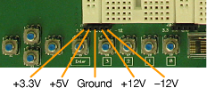
To provide power to the distribution strips, jumpers must be run from the strips to the five-position headers located below each distribution strip. The headers provide access to the labkit's ground, 5V, and 3.3V busses. Additionally, +12V and -12V are provided. The 12 volt busses employ linear regulators, for reduced noise. A self-reseting polycrystalline fuse limits the current drawn from each bus to 1A per bus. Should one of the fuses trip, the fuse will reset itself as soon as the load is removed.
Clocks
A 27MHz oscillator is built into the labkit PCB. This oscillator is connected directly to the FPGA, and is accessible via the signal clock_27mhz.
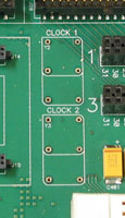
Additionally, two sockets are provided, each of which can accept a full- or half-can oscillator. Any oscillator that can operate at 3.3V can be used. Be careful to install oscillators in the correct orientation: the correct orientation is marked on the board. (Note the square corner, in the upper-left corner of the socket). The outputs of the two oscillator sockets are accessible via the signals clock1 and clock2.
Sockets for user-provided oscillators
Switches and Buttons
The labkit includes eight slide switches and nine momentary pushbutton switches. All of the switches are wired directly to the FPGA.
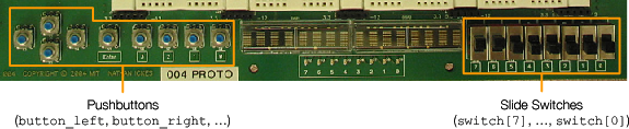
The 8-bit switch signal in the labkit.v file corresponds to the eight slide switches. Each bit of this signal will be a '1' when the corresponding switch is in the up position, and a '0' in the down position.
Four of the pushbuttons are arranged as an up/down/left/right keypad. The remaining buttons are designated "Enter", "0", "1", "2", and "3". The pushbuttons are represented by the signals button_up, button_down, button_left, button_right, button_enter, button0, button1, button2, and button3. The buttons use negative logic, so the above signals are normally '1', and change to '0' when the corresponding buttons are pushed.
Note that none of the switches or buttons are debounced.
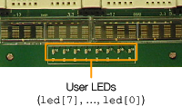
LEDs
There are eight discrete LEDs on the labkit, which are controlled by the led[7:0] signal in labkit.v. Driving a "0" to a bit in this signal will turn the corresponding LED on; driving a "1" will turn the LED off.
General-Purpose FPGA I/O
Four banks of 32 signals are provided for general purpose I/O, such as connecting to devices on the breadboards. These I/O banks correspond to the bidirectional (inout) signals user1[31:0] through user4[31:0].
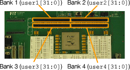
The 32 I/O signals in each bank are present on the bottom row of each connector. The top row of each of each connector is composed entirely of ground connections.
Although the actual I/O pins of the FPGA use 3.3 volt signaling levels, the user I/O banks are 5 volt tolerant. A pass transistor between the user I/O connectors and the FPGA clamps inputs higher than 3.3 volts, so that only 3.3 volts appears at the FPGA I/O pin. When used as outputs, the user I/O pins will only drive 0 volts or 3.3 volts: fortunately, most 5 volt logic devices will accept 3.3 volts as a logic 1.
Be careful using 5 volt logic. Only the user I/O signals are 5 volt tolerant: applying 5 volt to any other FPGA I/O pins (such as the logic analyzer or daughtercard signals) could damage the FPGA. Also, when working with 5 volt signals, be particularly careful to avoid contention (such as having the FPGA drive a pin to 0 volts at the same time that external logic is trying to drive it to 5 volts).
Logic Analyzer Connectors
Connectors are provided to interface to four pods of a Tektronix or Agilent logic analyzer. Each pod has 16 data signals and one clock signal.
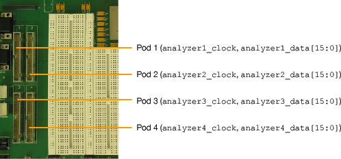
Each pod has a clock signal (analyzerN_clock) and a 16-bit data bus (analyzerN_data[15:0]). On Agilent logic analyzers, some triggering mechanisms only work with the dedicated clock input signal. On Tektronix analyzers, the clock input is no different from the 16 data inputs.
The logic analyzer connectors on the labkit are something of a compromise between the Agilent and Tektronix probes. An adapter cable is necessary to plug in either type of probe. Unfortunately, these adapters are not yet available. fortunately, the adapter for Tektronix analyzers does not contain any important circuitry. It is therefore possible to connect a Tektronix analyzer to the labkit using flying probe lead sets, by connecting to individual contacts in the logic analyzer connectors. The illustration below shows the pinout
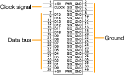
The clock and data signals for each logic analyzer pod are wired directly to the FPGA. In order to probe signals on the breadboard, it is necessary to route those signals into one of the FPGA user I/O connectors, and then program the FPGA to mirror those signals onto one of the logic analyzer ports. The buffers in the FPGA will, of course, add some small delay, but this delay should be negligible at clock speeds lower than 20MHz (and breadboarded logic is likely to run much slower than that anyway). If you really care about precise timing when probing signals on the breadboard, be sure to set timing constraints on the paths from the user I/O connectors to the logic analyzer outputs of the FPGA (or, just use the flying probe leadsets to probe breadboard signals directly).
Inter-kit Cable Connector
The labkit includes one 50-pin connector, which can be used to connect multiple labkits together with a 50-pin ribbon cable.
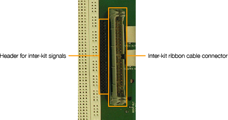
Every other conductor on the ribbon cable is connected to ground, to ensure food signal integrity. Thus, only 25 conductors are available for user signals. The 25 signal contacts from the ribbon-cable connector are connected to the nearby double-row header. Each row in this header corresponds to one signal on the ribbon cable. (The left and right contacts on each row are the same.) The ribbon-cable connector is not connected to the FPGA at all: to drive one of the ribbon-cable signals from the FPGA, route the FPGA signal to one of the user I/O connectors, and run a wire from the user I/O connector to the header near the ribbon-cable connector.
MIT 6.111 Introduction to Digital Systems, Updated April 05, 2005