|
|
|

for 6.111 Introduction to Digital Systems
6.111 home → Labkit home → Getting Started with ISE
Getting Started with ISE
by Nathan IckesIntroduction
The Xilinx Integrated Software Environment (ISE) is a powerful and complex set of tools. The purpose of this guide is to help new users get started using ISE to compile their designs. This guide provides a very high-level overview of how the tools work, and takes the reader through the process of compiling. The ultimate reference to ISE is of course the official documentation, which is installed on every PC in the lab, and is available from the Xilinx website.
From HDL to FPGA
The process of converting hardware design language (HDL) files into a configuration bitstream which can be used to program the FPGA, is done several steps.
First, the HDL files are synthesized. Synthesis is the process of converting behavioral HDL descriptions into a network of logic gates. The synthesis engine takes as input the HDL design files and a library of primitives. Primitives are not necessarily just simple logic gates like AND and OR gates and D-registers, but can also include more complicated things such as shift registers and arithmetic units. Primitives also include specialized circuits such as DLLs that cannot be inferred by behavioral HDL code and must be explicitly instantiated. The libraries guide in the Xilinx documentation provides an complete description of every primitive available in the Xilinx library. (Note that, while there are occasions when it is helpful or even necessary to explicitly instantiate primitives, it is much better design practice to write behavioral code whenever possible.)
In 6.111, we will be using the Xilinx supplied synthesis engine known as XST. XST takes as input a verilog (.v) file and generates a .ngc file. A synthesis report file (.srp) is also generated, which describes the logic inferred for each part of the HDL file, and often includes helpful warning messages.
The .ngc file is then converted to an .ngd file. (This step mostly seems to be necessary to accommodate different design entry methods, such as third-part synthesis tools or direct schematic entry. Whatever the design entry method, the result is an .ngd file.)
The .ngd file is essentially a netlist of primitive gates, which could be implemented on any one of a number of types of FPGA devices Xilinx manufacturers. The next step is to map the primitives onto the types of resources (logic cells, I/O cells, etc.) available in the specific FPGA being targeted. The output of the Xilinx map tool is an .ncd file.
The design is then placed and routed, meaning that the resources described in the .ncd file are assigned specific locations on the FPGA, and the connections between the resources are mapped into the FPGAs interconnect network. The delays associated with interconnect on a large FPGA can be quite significant, so the place and route process has a large impact on the speed of the design. The place and route engine attempts to honor timing constraints that have been added to the design, but if the constraints are too tight, the engine will give up and generate an implementation that is functional, but not capable of operating as fast as desired. Be careful not to assume that just because a design was successfully placed and routed, that it will operate at the desired clock rate.
The output of the place and route engine is an updated .ncd file, which contains all the information necessary to implement the design on the chosen FPGA. All that remains is to translate the .ncd file into a configuration bitstream in the format recognized by the FPGA programming tools. Then the programmer is used to download the design into the FPGA, or write the appropriate files to a compact flash card, which is then used to configure the FPGA.
Template Design Files
In order to interact with any of the codecs, memories, or even general I/O pins on the labkit, the I/O ports defined in the top-level Verilog module of a design must be mapped to the correct I/O pins on the labkit's FPGA. This is done by means of constraint statements inside a universal constraints file (.ucf).
The FPGA used in the labkit has 684 I/O pins (and most of them are actually connected to something on the labkit PCB!) It would be extremely laborious to type out the necessary constraints for each new project, so, to simplify the process of adding pin constraints to a new design, two template files have been developed.
labkit.vis a template top-level Verilog module. This module defines names for all of the signals going in or out of the FPGA. Additionally, it provides default assignments for all FPGA outputs, so that unused circuits on the labkit are disabled.labkit.ucfis the standard constraints file for the labkit. This file contains constraint statements that tie the signals inlabkit.vto the appropriate physical FPGA pins.
The labkit.v should be used for the top-level module of every labkit project. You will have to modify this file to instantiate your own design within it.
An ISE Tutorial
- Download the following source files: the standard toplevel template module (
labkit.v), the standard labkit constraints file (labkit.ucf), and the sample counter design for this tutorial (counter.v). - Launch the Project Navigator application (Start → Programs → Xilinx ISE 8.2i &rarr Project Navigator).
- Select "New Project" from the "File" menu
- Enter a project name and choose a project location. Be sure the top-level source type is set to HDL (hardware design language). Click the "Next" button.
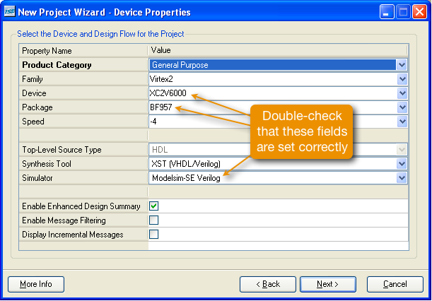
- On the second form, enter the target device information. The FPGA on the labkits is a Virtex 2 family XC2V6000, speed grade 4, in a BF957 package. Select "ModelSim-SE Verilog" as the simulator.
- The next form allows you to create a new source file and automatically add it to the new project. Note that there is really no reason to create a new source file when creating a project: you can create a new source file and add it to the project at any time. Since you have already downloaded all of the source files needed for this tutorial project, just click the "Next" button.
- The following form allows you to add any existing source files to the new project. Add the
labkit.v,counter.v, andlabkit.ucffiles you downloaded earlier, as shown below.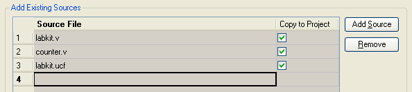
- Click "Next" to advance to the project summary form, and then click "Finish" to create the project. When the "Adding Source Files..." dialog pops up, click "OK".
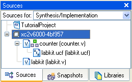
- Once ISE has created the new project, the "Sources in Project" tree in the Project Navigator window should look like this:
Modifying the labkit.v Template
- To instantiate the counter module in the top-level
labkitmodule, openendmodulestatement.wire [31:0] count; counter counter1 (.clock(clock_27mhz), .count(count)); assign led = ~count[31:24];
After saving the file, note that the project hierarchy tree changes to show that thecountermodule is now a submodule oflabkit.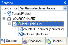
- The stock
labkit.vfile assigns a default value to the LED outputs. In order to drive the LEDs with thecountermodule, we need to delete the following line, which can be found near the end oflabkit.v.assign led = 8'hFF; // Turn off all LEDs
- The stock
Compile the Design
- The
labkit.ucffile includes constraints for all of the input and output ports defined inlabkit.v. Most designs, however, will not use all of these signals, in which case the synthesis engine will optimize the unused signals out of the design. The location constraints inlabkit.ucffor these unused signals will then generate errors. It is therefore necessary to tell ISE not to generate an error if it encounters a pin constraint for a (now) nonexistent signal. To do this, right-click on the "Implement Design" item in the process pane, and select "Properties...". Check the box to "allow unmatched LOC constraints" in the "Translate Properties" form, as shown below.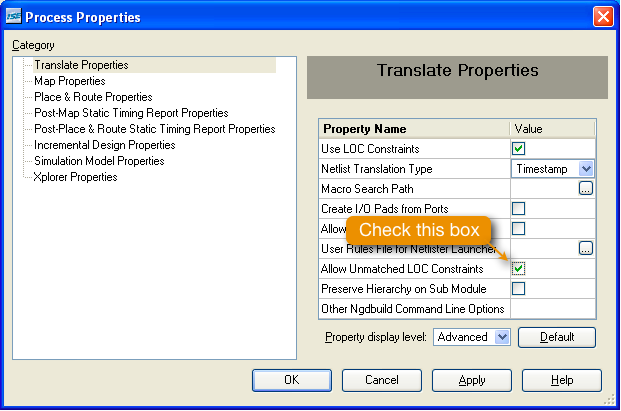
- Make sure the top-level
labkitmodule is selected in the project source tree. - Double click "Generate Programming File" in the tasks area of the Project Navigator window.
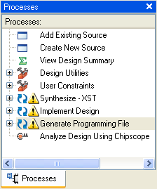
This will cause the "Synthesize", "Implement Design" and "Generate Programming File" tasks to be run in order. It's normal with this design for each stage of the compilatio to produce warnings, so a yellow triangle will appear beside each task when it is successfully completed. It will take a couple minutes for everything to complete.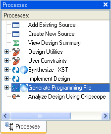
Downloading the Compiled Design to the Labkit Hardware
Once you have successfully run the "Generate Programming File" task, read the configuration methods tutorial to learn how to download the compiled design to the actual labkit.
MIT 6.111 Introduction to Digital Systems, Updated February 04, 2007