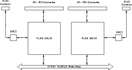
Figure 1: FPGA Module Block Diagram
The FPGA module consists of two of Altera's FLEX 10K PLDs, one FLEX 10K10 and one FLEX 10K70, which can be accessed through the lab kit's NuBus interface and 50-pin ribbon cable connectors. The state of the NuBus interconnects can be continuously displayed on the lab kit's hex leds by connecting jumpers /LHEX and /HHEX to /CLK (or any other clock). Also, the Proto strip connection labeled NUHEX must be grounded.

Figure 1: FPGA Module Block Diagram
The 50-pin ribbon cable connectors can be fed directly into the inputs
of the Logic Analyzer via 50-pin connectors on the kit.
Note that each gate array has its own 50-pin connector which can be
connected either to the K1 or K2 connectors on the kit.
BEWARE, the signals which are grounded by the K1 and K2 connectors are
different!
It is never a good idea to use EDGEs of signals on the 50-pin
connectors.
Use only ``levels'' and wait for the ringing to settle down before
sampling them.
Most of the NuBus connections to the FPGA are to I/O pins, but
one is a clock pin.
Both gate arrays are driven by the same clock.
Note that A31 is used for supplying the clock to the CPLD module if
one is also used. Thus this should not be used by either FPGA if a
CPLD board is used.
Information on the Flex devices can be found on Altera's web site.
The URL is http://altera.com/products/devices/flex10k/f10-index.html.
From there, you can click on Data Sheets and find
http://altera.com/literature/lit0f10.html and then click on the first
data sheet. This tells you more than you want to know!
Please don't print it out unless you really want to save the paper
copy - it is 128 pages long! Pages 5 through 15 give you a good
summary of capabilities.
This data sheet tells you that the
10K10 has 10,000 gates and 576 logic elements while the 10K70 has
70,000 gates and 3744 logic elements.
That is a lot of capability.
Even badly written VHDL code is likely to fit!