Introduction
The purpose of this memorandum is to describe general requirements for the
reports you must write for laboratory exercises and for the final project. It
also describes how 6.111 is a (CI-M) Communications Intensive Subject.
Good writing is more important than many of you think. The documents you
produce are the principal way of communicating your work. Well-written reports
reflect well on your work and on you. Badly written documents, on the other
hand, will produce negative impressions, even if those documents represent very
good technical work. It is worth the effort to pay careful attention to your
writing.
A well-written document contains more than clear language, correct syntax,
grammar and spelling. It must also reflect clear thinking. Particularly with
documents such as those you will produce in 6.111 (dealing with complex
technical issues), it is important that care be taken to ensure that the writing
clearly and accurately describes the topic. Pictures such as wiring and timing
diagrams should be incorporated into the text and be clearly described both in
the text and in the captions.
CI-M Considerations
6.111 is a CI-M subject. Lab reports 1, 2, and 3, as well as each
individual's part of the project report, will be graded for writing style and
clarity, as well as for technical content. The report for Lab 2 has a required
revision. You will receive detailed comments on technical content and writing
style and have adequate time to make a revision which will then be graded.
Report Style and Audience
Write for your colleagues. You should assume an audience with
technical capabilities similar to your own. It should be possible for other
students and for faculty to understand your report. Thus you can assume general
technical knowledge on the part of your reader. You should not assume that your
reader has a lot of specific knowledge about your subject area.
Write for yourself. A careful job of documenting your work can help
you to organize your project. This can be particularly helpful if done early in
the project. Your own carefully thought out explanation of how each element of
your circuitry works can help in the process of design. Describe the function of
each element and how the elements work together. Then think about what you have
written. A surprising number of design errors can be discovered by this process,
even before you start writing HDL (VHDL or Verilog) code or wiring.
Organize your work carefully and do a neat job. Each of the reports should be
typed. Powerful word processing tools are readily available to students in
6.111. Use them. Figures should be done on a computer graphics system or drawn
with drafting aids (template and straight-edge). Lettering on figures can be
done by hand, but must be neat and legible.
Remember to leave yourself enough time to do the report properly. Proofread
your report! Eliminate typographical and spelling errors. Remember, your report
is representing you to the world (and to the good folks who determine your
grade!).
Organization
Your reports should be long enough to fully describe your work, but no
longer. We expect that your reports for Labs 2 and 3 will be perhaps ten or
twelve pages long, not counting front matter, back matter, or graphics. The
project proposal document should be only a few pages, but the project report
will probably exceed twenty pages (in some cases by a substantial amount). Your
report should include schematic, timing, and state diagrams and other figures,
where appropriate. These pictures, with appropriate descriptions, will help to
make your report clearer.
Term projects in 6.111 are team efforts. You will be working with one or two
other students to build a (hopefully) working system. It is usually appropriate
for project teams to submit a joint report. This is permitted (but not
required), but it is important that the work of each student be clearly labeled.
Your reports should have the following parts:
Title and Abstract
Table of Contents
List of Figures
Overview
Description
Conclusions
Appendices
In the title, identify the device that you have created. Avoid such deadwood
as ``Report on'' or ``Specifications of''. The abstract, which should appear on
the title page, is a one-paragraph description of your project. The same
abstract may appear in both the project proposal and final report, or it may be
necessary to modify the abstract to reflect changes in scope or direction after
the proposal.
If the report has joint authorship, the Table of Contents should disclose the
authorship of different sections.
Style Considerations
Accuracy and Completeness:
Be sure that your report accurately and completely describes your work. One
of your colleagues (fellow students, teaching assistants or faculty) should be
able to understand what you have done and to, on the basis of your descriptions,
reproduce your work.
Well-organized, logical structure:
Each section of the report should state an objective, provide examples and
reach a conclusion. The paper should proceed systematically; and transitions
from each section, paragraph and sentence to the next should be smooth and
coherent.
Appropriate language and tone:
Technical terminology will, of course, be used, but you should avoid jargon.
Write simply and clearly. Use the simplest language available to convey your
meaning.
Correct grammar, spelling, punctuation and capitalization:
Proofread carefully. Rid your paper of little bugs.
Thoroughness:
Do not assume that your reader already knows what you are writing about. You are not taking a quiz. Avoid answering questions with:
Part B) 30 nanosecondsWhat does that mean? How did you measure it? Without the lab handout, someone reading this does not know what this measurement refers to. Describe what you measured, how you measured it, what calculations (if any) were involved in arriving at this answer. Describe logic analyzer or oscilloscope traces if appropriate.
Thoroughness also means including all the necessary pieces in your lab
report. If you program a FPGA, PAL, or EPROM, you must include the programming
files (VHDL files, dat files, etc.). Most of the time it is appropriate to put
these computer printouts in an appendix.
Always fully document any ``non-standard'', clever or ``hack'' mechanisms. It
will help others to understand your design, as well as remind you why you built
that thing that way in the first place.
Overview (1 - 2 pages)
The most important rule of thumb for organizing a technical description is ``Describe the whole before the parts''. This rule is based on the assumption that the device which you are describing is unknown to the reader and that a general view of the purpose and construction is needed before the details can be understood.
With this rule in mind, start your 6.111 report with an overview of the
purpose, use and design of the device, what a user does with it and how he or
she would do it. Describe in general the subsystem organization of the device.
Emphasize those internal features which implement the main user-visible
features.
Description (5 - 7 pages)
The device must be described in enough detail for a skilled engineer to understand how it works and to enable him or her to reconstruct it. This function is the heart of any technical description.
This description normally includes the project functional specifications, the design used to implement these specifications and a detailed description of how the design works. Descriptions are usually organized in a way that mirrors the design of the device. Thus, there is a separate subsection for each module. A useful criterion for ordering the subsections is the flow of information (input to output) within the device as a whole. When this criterion is not applicable, it often suffices to specify more important modules before less important ones.
Your 6.111 project report has the special requirement that each subsystem be described by the partner who is responsible for it. Thus, use a sub-heading to identify the subsystem and the modules within subsystems. Use this sort of organization:
Subsystem 1 (by Richard Francis Burton)Normalizing Shift ModuleSubsystem 2 (by Alistair Cooke)
Master Control ModuleRule-Interpreter Module
RAM-Control Module
Analog Conversion Module
Include at least one-sentence introductions at each level (e.g., ``The device consists of two subsystems which ...'').
Illustrate the descriptions with the block diagrams that you prepared earlier
in the project (you may want to re-draw them). Add any tables or figures that
help clarify your description. Refer to these by figure or table number. Be sure
to label units of measure unless it is absolutely clear to everyone what they
should be. Detailed logic diagrams usually belong in an appendix.
Testing and Debugging (2 or 3 pages)
Very infrequently will something you have built actually work the first time
you turn on the power. Testing and debugging are natural parts of the
engineering process. If your circuit is comprised of several smaller subsystems,
you should include a description of how you tested each one after you
implemented (programmed or built) it. If a subsystem did not work as you had
planned, give an overview of the debugging steps that you followed to make it
work. In the worst case, if you just could not get a lab project working,
describe which subsystems worked and to what extent. You should also indicate
what the remaining problems and obstacles were and what your next testing and
debugging steps would have been to solve those problems.
Conclusion (1 - 2 pages)
The conclusion of a project report typically summarizes the most important or
innovative design features. The conclusion also often suggests ways in which the
design could be improved. In your 6.111 report you should also make a point of
summarizing the test results. If these were not fully satisfactory, they provide
a natural basis for suggesting improvements. As a guide to others, it is very
helpful to include some discussion of the problems you met in your initial
design and what you did to overcome these problems.
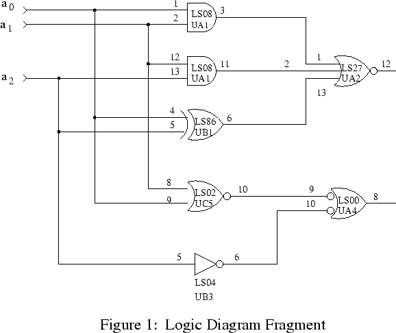
Circuit Diagrams
Circuit diagrams help convey information about a piece of design work you have accomplished and implemented. Learning to ``speak the language'' of circuit diagrams will facilitate getting your ideas across to others and make things easier to build and debug.
Points to remember:
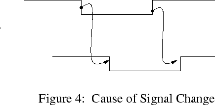
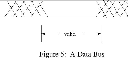
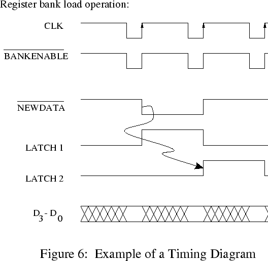
Timing Diagrams
Timing diagrams demonstrate that the signals within a system behave in an orderly fashion to achieve a design goal. They show the cause and effect relationships between signals.
Points to remember about timing diagrams:
Figure 6 shows an example of a timing diagram.
Donald E Troxel 2003-09-09