
| Distributed: 3/19/97 | Due: 4/4/97 |
In this lab, you will learn the basics of hardware design with massive regular structures. Although the abstraction of reconfigurable regular structures is elegant, it is a difficult problem to build testable, reliable, and efficient computation structures out of regular structures. You will get a taste of the practical engineering tradeoffs, such as speed versus area, and compilation efficiency, faced in implementing computational functions.
Goals of this lab:
There is a trend in industry toward the use of reconfigurable regular
structures, such as FPGAs, in hardware design and prototyping. When compared
to the traditional method of hardwired prototyping on PC boards or breadboards
using discrete logic functions, design and prototyping with FPGAs is quicker,
cheaper, and less risky. Modern FPGA design tools allow engineers to functionally
simulate their designs before implementation; this allows designers to
catch bugs before implementation in physical hardware. FPGAs also offer
a greater net density per board area of hardware, which helps keep manufacturing
costs down. Finally, the type of FPGA used in this lab is in-circuit configurable,
which means that even after the physical hardware has been built, you can
fix bugs in the FPGA and reprogram it in a matter of seconds. It also means
that the same piece of hardware can be configured to do many tasks. This
lab will provide an introduction to this technology.
This lab requires no components. You will, however, need the Xilinx Foundation Series design software. It is available via ftp to cs00.mit.edu. Details on how to retrive and install this software were distributed via email, and they are not repeated here for security reasons. If you do not have access to a machine that can run this software, you may come to lab and use the HP Mongoose PCs.
Implementing a device as complex as a 32-bit RISC microprocessor is a non-trivial task (ask your sophomore friends at other colleges and see if they've tried it). The approach taken in 6.004 to implementing the Beta microprocessor is a structured, implementation driven bottum-up approach. In other words, high-level design decisions are made in consideration of the underlying implementation hardware, and then the hardware is implemented and tested in small modules. This section of the prelab will famaliarize you with the implementation hardware (also known as the "target").
The Field Programmable Gate Array (FPGA) is a class of massive, reconfigurable regular structure. As you may recall from the problem sets and lectures, PLAs consist of a large programmable AND-OR plane capable of implementing huge sum-of-product functions; this is an example of a coarse-grained architecture. FPGAs generally have a fine-grained architecture. Instead of a single huge logic plane, FPGAs use many small logic blocks with programmable interconnections between them. Packaged with each logic block is a flip flop of some kind so one can design sequential circuits.
The FPGA targetted by the designs in this lab is the XC4013E. It is manufactured by Xilinx, and it is capable of implementing up to 13,000 gates of logic and 1,536 flip-flops. The majority of the reconfigurable hardware in the 4013E can be classified as one of the following:
There are 576 configurable logic blocks in the XC4013E. This is where the majority of the combinatorial logic and flip flops reside. These CLBs have a structure as follows:
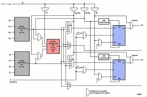
Although this seems complex, its structure can be boiled down into a few key parts:
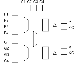
The key I/O "pins" of the CLB are F1-4, G1-4, C1-4, YQ, XQ, Y, and X. The F, G and C pins are inputs, while YQ, XQ, Y, and X are outputs. YQ is a registered version of Y, and XQ is a registered version of X. A CLB can be abstracted into a black box as follows:
The schematic depiction above includes two extra symbols-the triangles on the right hand side-which indicate the fact that each CLB also has 2 tri-state output buffers. These tristate buffers allow users to implement wired-OR logic and internal multi-driver busses.
CLB Utilization Exercises
The following series of pre-lab questions will help you become familiar with the limitations and strengths of the CLB. You need not provide detailed answers--the point is to get you thinking about how different functions map to CLBs in terms of scalability, speed, and area efficiency.
Combinatorial Logic and the CLB
What is kinds of functions can be implemented by a single CLB? In the space below, determine the largest multiplexer you can implement with a single CLB. How would you implement it using the above structure? Can you implement a one-bit full adder with a single CLB? How about a 2-bit full adder? What size ROM could you implement in a CLB? How come you cannot implement a 2-4 decoder in a single CLB? Note the strong bias of this structure toward n-to-1 logic functions, as opposed to 1-to-n logic.
one-bit full adder: yes / no
two-bit full adder: yes / no
size of ROM: ______ x ______ bits
Reason why you cannot implement a 2-4 decoder:
One way of implementing large multiplexers is to use the tristate buffers instead of a heirarchy of FMAPs. Sketch an 8-1 mux using FMAPs, and then sketch an 8-1 mux using tristate buffers. You need not provide any detail--just indicate clearly the number of CLBs you would need and the propagation delay of your two mux implementations.
Sequential Logic and the CLB
What is the largest state machine in terms of the number of inputs and the number of states you can implement using a single CLB, assuming that two of the inputs to the CLB are used to provide state feedback?
Number of inputs:___________
Number of states:___________
Can you implement a 2-bit counter in a single CLB? How about a 2-bit accumulator? You may assume that outputs can be routed to inputs to provide a feedback path.
2-bit counter: yes / no
2-bit accumulator: yes / no
How might you use multiple CLBs to implement an OR gate with 16 inputs? Assume that you have total connectivity between CLBs. Assuming that each CLB has a propagation delay of tpd, what is the total delay of your implementation?
Note that a CLB also has another mode where it can be configured to function purely as a memory element. A single CLB can implement both edge-triggered and level sensitive memory devices with sizes of 16x1 dual-port, 16x2, or 32x1 bits. In this mode, the function generators (FMAPs and HMAPs) are used as RAM storage devices. You will use these memory modes in lab 5 to implement the register file and control logic of the Beta.
In order to get signals onto and off of the chip, special blocks are provided called Input/Output Blocks (IOBs). There is one IOB per I/O pin; an XC4013E has 192 I/O pins in the 240-pin package that is used in your lab kit. The remaining pins are dedicated to configuration, control, power and ground.
In order to make your design useful, you have to explicitly declare I/O cells in your design. If you do not declare I/O pins, then the logic optimizer will optimize out all unconnected logic.
The IOB has a structure as follows:
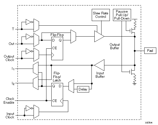
The key features of the IOB are:
IOB Questions
Why do you suppose the output buffers have a programmable slew rate option? Think back to the lecture on transmission lines and power and ground lead inductance.
What is the purpose of the input delay option? Think about the impact this may have on the hold time of the input flip flop. What kind of problem might arise if this delay element was not provided?
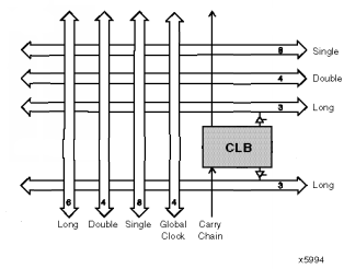
Connecting all 576 of the CLBs and 192 of the IOBs together is a difficult problem. Xilinx' answer to this problem is its programmable interconnect architecture of manhattan wires and switch matrices. The programmable interconnect runs in between the CLBs, which are arranged in an array of 24x24 blocks.
Each CLB can route to:
Single-length lines allow CLBs to connect to directly adjacent blocks and no further; double length lines allow CLBs to connect to blocks that are up to two blocks away, and the longlines connect all 24 blocks in a vertical or a horizontal stretch. The global clock lines connect to all 576 of the blocks in the device, and it is used to provide a low-skew distribution network for critical nets such as clocks. There are also two special vertical lines running between each CLB in a column to provide a fast path for carry signals (such as those required in addition).
At the intersection of horizontal and vertical wires, MOSFET switches are provided to increase connectivity. Each MOSFET switch has 1 bit of static RAM associated with it which configures whether the switch is open or closed. These RAM cells are initialized during device configuration.
The following diagram illustrates the local connectivity available to each CLB:
And the following diagram illustrates the topology of the single and double length lines, along with the programmable switch matrices:
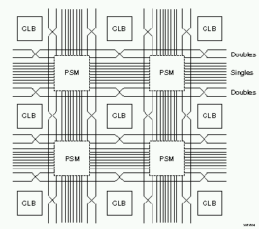
The following diagram is the simplified internal structure of a PSM:

Each pass transistor that a signal is routed through adds some delay to the signal; the actual wires on-chip also have a non-negligible delay. Thus, the delay of a signal routed through the programmable interconnect can vary depending on the distance it has to travel and the number of pass gates it must go through. In fact, the cumulative delay of the signal routing alone can easily exceed the combinatorial delay of a single CLB (typ. 4 ns). The autorouter uses a random search algorithm known as simulated annealing to place wires, and thus the same design can have different critical paths each time it is compiled. This is one of the least attractive features of the 4013E architecture, because it makes creating a reliably fast design very difficult.
It turns out that despite the seeming plethora of routing resources, the limiting factor in most designs is still the lack of connectivity between CLBs. In order to guarantee the routability of an FPGA design, the design should utilize around 80% or less of the available CLBs.
Programmable Interconnect Questions
Think about the factors that contribute to the routability of a design. What kinds of functions map well into a routing topology such as the 4013E's? What kinds of functions map poorly into this routing topology?
How well does this routing topology scale? In other words, is this topology optimal for logic arrays of any size? Why or why not?
Thus, the overall picture of the 4013E FPGA you are using in the lab looks as follows:

Hopefully, you now have a better picture of how FPGAs work, and what they are like on the inside. This knowledge is required to design an efficient and routable Beta microprocessor.
Now, the question of how can one design a circuit for such a complex device without having to specify every logic map and interconnect must be answered. There are many approaches to the design of reconfigurable logic; some involve using text-based languages such as VHDL. The approach used in 6.004 is based on a schematic capture process. Although this process is not as popular in industry today due to some of its limitations and lack of portability, it is still the easiest to learn.
In order to isolate the designer as much as possible from having to specify the contents of FMAPs, HMAPs, and programmable interconnects, the schematic tools provide the ability to instantiate and create heirarchical macros. For example, one has to specify at the gate or FMAP level a 1-bit full adder only once. Once a symbol for the adder has been built, one can use it as if it were a primitive part. So, building an n-bit full adder requires you to instantiate n 1-bit full adder symbols instead of gobs of FMAP logic. You will make extensive use of heirarchical macros in this lab to build the Beta ALU. In fact, the design tools provided for you comes with a huge library of macro parts.
The process of translating a schematic to a configuration bitstream is quaintly referred to as compilation. A configuration bitstream is a binary image of the state of the programmable interconnect switches and the CLBs. The compilation process can be broken down as follows:
Schematic -> Netlister -> Translation -> Optimize -> DRC -> Mapping -> Place -> Route -> Bitstream
Simulation
Once a design is compiled and uploaded into a chip, it is essentially a black-box abstraction. You cannot probe the chip in any way; the only means for finding bugs is through signals brought out to the pins. Because of this difficulty and because of the complexity of designs typically implemented in FPGAs, functional simulation is a necessity.
"Functional" simulation implies that system timing is not a part of the simulation. In other words, in a functional simulation, all setup and hold times are assumed to be met, and combinatorial delays are negligible. Instead, one focuses on whether or not their logic is correct.
Because of the compilation-dependant nature of the on-chip timing of these parts, it is in fact pointless to attempt to simulate timing before compilation. Also, compilation is a long process-on the order of hours for complex designs-so timing analysis is only done after functionality has been verified.
In this lab, you will build a Beta ALU and perform a thorough functional simulation. This will give you a reliable ALU macro that you will eventually use to implement the Beta.
Before attempting to build the ALU, read over the Beta Instruction Set Architecture Reference and the Beta Executive Summary handed out in lecture. Not all the material in those documents is covered here, but they are essential to do the lab. Familiarize yourself with the basic unpipelined Beta architecture; you have to know what you are implementing before you try to build it!
In order to figure out what we need inside the ALU, we have to look at the Beta specification. In particular, check out the instruction set, reproduced here:
| 000 | 001 | 010 | 011 | 100 | 101 | 110 | 111 | |
|---|---|---|---|---|---|---|---|---|
| 000xxx | ||||||||
| 001xxx | ||||||||
| 010xxx | ||||||||
| 011xxx | LD | ST | JMP | BEQ | BNE | LDR | ||
| 100xxx | ADD | SUB | mul* | div* | CMPEQ | CMPLT | CMPLE | |
| 101xxx | AND | OR | XOR | SHL | SHR | SRA | ||
| 110xxx | ADDC | SUBC | mulc* | divc* | CMPEQC | CMPLTC | CMPLEC | |
| 111xxx | ANDC | ORC | XORC | SHLC | SHRC | SRAC |
Don't worry about the actual instruction numbers yet -- the translation will be handled by the control logic you build in the next lab. Instead, let's look at the different types of arithmetic and logic we need to do.
| FUNCTION | INSTRUCTION MNEMONIC |
|---|---|
|
addition |
LD, ST, LDR, ADD |
| subtraction | SUB |
| comparisons | CMPEQ, CMPLT, CMPLE |
| logical and | AND |
| logical or | OR |
| logical xor | XOR |
| barrel shifting | SHL, SHR, SRA |
| pass a value | LDR, BEQ, BNE |
"Pass a value" for LDR, BEQ, and BNE means to simply make the output equal to one of the inputs (A). These instructions require the value of PC+4+(C<<2) and uses it as an address, and the Beta computes the value of PC+4+(C<<2) outside the ALU. Why isn't this done in the ALU itself? It turns out there is a good reason for this.
A barrel shifter shifts a 32 bit number by an arbitrary number of bits to the right or left.
Comparisons return the value 1 if A is =, <, or <= B for CMPEQ, CMPLT, or CMPLE, respectively, and they return the value 0 if the condition isn't true. In reality, the ALU performs a subtraction, and uses some logic to figure out whether the result is positive or negative.
Note that the ALU makes no distinction between instructions that call for values from the register file or from the constant field of the instruction. This is because the logic which selects Rb or the constant is outside the ALU.
Please refer to the Beta Instruction Set Architecture Reference passed out in lecture for all the nasty little details. You will need to know the details to do this lab.
The schematic capture tool is set up for a heirarchical design. In other words, you can make a circuit, then define input and output pins, and turn the circuit into a box that you can use on higher-level circuits. This abstraction helps keep your schematics uncluttered, allows you to do a bottom-up or top-down design, helps with bug fixes, etc. All the preaching you got in 6.001 about encapsulating simple pieces of code into functions applies here to hunks of circuitry.
The top-down design of the Beta has already been presented in class. A bottom-up strategy (small pieces first that get hooked together) is used when we actually build the hardware so that we can test small parts to make sure they work before burying them in a mass of other circuitry.
A set of library macros have been created to expedite ALU design. The full list of parts that you can use for this lab include:
| ADSU32 |  |
A 32-bit wide adder/subtracter. This part has A and B bus inputs, and a single bit specifying whether you want it to add or subtract. The output is 32 bits wide. The carry out bit is not available. |
|---|---|---|
| AND32 | A 32-bit wide two-input AND gate | |
| OR32 | A 32-bit wide two-input OR gate | |
| XOR32 | A 32-bit wide two-input XOR gate | |
| MUX32 | A 32-bit wide two-input multiplexor. A single input connects one of two input busses to the output bus. An input of 0 selects the A side. An input of 1 selects the B side. | |
| OR32_1 | A 32-bit wide or gate. This takes a bus that is 32 bits wide and spits out a single bit that is the OR of all the inputs. Use this to determine whether a bus is carrying the number zero. | |
| EXP16 | Expand (copy) a single bit to a 16-bit wide bus. You may find this handy in your barrel shifter. | |
| EXP32 | Expand (copy) a single bit to a 32-bit wide bus. Useful for providing a bus of all-zeros or all-ones. | |
| BUFE32 | 32-bit wide tri-state buffer. The enable pin is active LOW. A tri-state buffer either connects its input pin to its output pin, or it completely disconnects the output alltogether. This is useful when you want to connect several outputs together, and you only want to have one of them active at a time. If more than one of the buffers is enabled (has a zero on the enable pin) at a time, you are in danger of letting the magic smoke out of your chip. |
You will use the MUX32 to create a barrel shifter. Once you have the barrel shifter working, you can string the rest of the parts together to make an ALU. The only tricky part about the ALU is the logic for the CMP instruction. If your ALU drawing gets too cluttered, or you just want the space, you can turn the CMP logic into another heirarchical module. In the next lab, you'll take the ALU you made and build the rest of the Beta around it.
Arithmetic Compares
The arithmetic compare of A < B is done by subtracting B from A and looking and the result.
Your buddy Ben Bitdiddle (the same guy from 6.001 who couldn't get anything right), claims that if A is less than B, then A-B will be negative, and all you have to do is look at the sign bit (bit 31) of A-B. Why isn't he right?
![]()
It turns out that figuring out the inverse of "less than" (which is "greather than or equal to") is easier than determining "less than". You can do it using the sign bit (bit 31) of A, B, and S, where S=A-B. Think about it very carefully; drawing out a truth table detailing all the possible combinations of positive and negative A and B, and the resulting value of S, will help you reason it out.
![]()
Fill out a Karnaugh map and figure out a gate implementation as well.
Boolean Logic Functions
In order to allow your Beta to fit on a single XC4013E device, a funky optimization is employed in the computation of boolean logic functions.
Instead of providing a computation structure for each of the logical functions, all three logic functions (AND, OR, and XOR) and the pass-through function are going to be computed by a single structure.
To understand why this is done, consider the following implementation approach for the Beta ALU:

Notice how each logic function is in its own separate world, sequestered by a tristate buffer. How would a single bit slice of a two-input, one-output logic function map into an FMAP? Since each of the 32 bits of computation are independant, we can assume that a 32-bit wide 2-input one output logic function will consume 32 times the number of FMAPs required to implement a single bit slice.
It turns out that the following structure yields a tighter implementation:
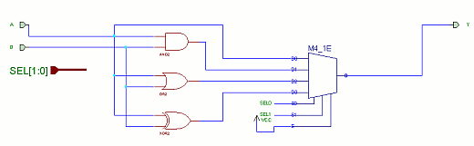
Convince yourself that this implementation works. The M4_1E symbol is a 4 to 1 multiplexer with enable (which, in this case, is tied active). Now, how many FMAPs are required per bit slice of combined AND, OR, XOR, and passthrough?
How many FMAPs are required to implement the full 32 bits?
Also, how efficient is this implementation in terms of using the full power of an FMAP?
How many FMAPs did you save by employing this optimization?
This kind of optimization is an example of how a high-level architecture choice can radically affect the low-level implementation efficiency.
First, some logistics. You will be building a single project from now until the end of the semester.
This part is pretty complicated, but you'll only have to do it once. Make sure you have a copy of the lab handy so you can get the steps right.

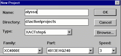
Now for the good stuff...
The foundation series schematic capture tool uses a connection by name scheme. In other words, what matters is the name of a bus connected to a pin, and not what the bus itself is connected to. In the case of a conflict between drawn bus connections and an explicit name, the explicit name will always have precedence. On the other hand, an unnamed bus will default to the name of whatever it is connected to.
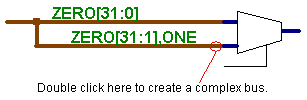
The picture above shows a special feature of busses that you might find
useful. To make this picture, draw the first (upper) bus and name it. This
bus has 32 pins and is called zero. To name a bus, click the bus icon (![]() ),
then click the wire naming tool (
),
then click the wire naming tool (![]() ).
Type the name of the bus, being sure to get the wire count right (31:0
makes 32 wires). The mouse will now have a rectangle attached to it. Click
on the bus to drop the label and name the bus. The second bus is attached
to the first one, and has a special label. We'll assume that there is a
wire somewhere else in the picture called "ONE". Double click
on the second bus, right near the pin of the mux. A special window will
appear with a single input box. Type "ZERO[31:1],ONE" (without
the quotes). This means that the new bus will have pins 31 through 1 of
the zero bus, followed by the value of the "ONE" wire.
).
Type the name of the bus, being sure to get the wire count right (31:0
makes 32 wires). The mouse will now have a rectangle attached to it. Click
on the bus to drop the label and name the bus. The second bus is attached
to the first one, and has a special label. We'll assume that there is a
wire somewhere else in the picture called "ONE". Double click
on the second bus, right near the pin of the mux. A special window will
appear with a single input box. Type "ZERO[31:1],ONE" (without
the quotes). This means that the new bus will have pins 31 through 1 of
the zero bus, followed by the value of the "ONE" wire.
You can use this feature to make your barrel shifter.
You will start building your Beta ALU by creating a symbol for it. Under the
A barrel shifter is a rather simple principle. Suppose we wanted to shift a string of bits 12 spaces to the right. One way to do so is to shift it 4 spaces to the right and then 8 spaces to the right. We get this from the binary number for 12, 0b1100, meaining 23+22 or 4+8.
To shift a 32-bit pattern any number of bits to the right, we need to make a 5 stage shifter. The first stage will either pass the number through or shift it 1 bit to the right. The second stage will either pass the new number through, or shift it 2 bits to the right. The third stage will choose between passing and shifting 4 bits, etc. The empty bits, of course, need to be filled. You should build a barrel shifter that lets the user specify the fill bits.
To be more concrete, your barrel shifter will have four inputs. One 32-bit input is the source number. The second 32-bit input is the number of bits to shift the source. Your barrel shifter will only use the bottom 5 bits of this number, but we'll take in a 32-bit number to make things easier for the next level up. The third input is a single bit to determine the fill. When this input is zero, the holes left by shifting the original number right or left will be filled with zeros. If the fill input is one, the extra slots will be filled with ones. The final input is a single bit controlling whether the shift should be to the right or left.
Internally, your barrel shifter will have two parts: a left-shifter and a right-shifter. Each shifter will have five MUX32 parts, and a bus structure that looks like the picture above. An eleventh MUX32 at the end will decide which track (left-shift or right-shift) ends up at the output. Your Fill bit will also need to be expanded into an F bus of 16 bits in order to fill all of the shifts.
To help you design the barrel shifter, write the labels you'll need to put on the special busses below. The first stage has been filled in for you.
| Stage 0 (1) | Stage 1 (2) | Stage 2 (4) | Stage 3 (8) | Stage 4 (16) | |
| Bus name | A | LB/RB | LC/RC | LD/RD | LE/RE |
| LEFT | A[30:0],F0 | ____________ | ____________ | ____________ | ____________ |
| RIGHT | F0,A[31:1] | ____________ | ____________ | ____________ | ____________ |
Don't forget that the pass-through bus in each stage must have a different name, or the schematic capture system will think they're all the same bus with the same values.
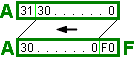 If you're
confused, the picture to the left may help. The upper box illustrates A[31:0].
This is just 32 bits of A, one after the other. The lower box shows the
output of Stage 0 Left, A[30:0],F0. Note how everything has been
shifted one bit to the left. A31 has fallen off the end, and F0 comes in
to replace it.
If you're
confused, the picture to the left may help. The upper box illustrates A[31:0].
This is just 32 bits of A, one after the other. The lower box shows the
output of Stage 0 Left, A[30:0],F0. Note how everything has been
shifted one bit to the left. A31 has fallen off the end, and F0 comes in
to replace it.
Test your barrel shifter by running the simulator and putting some sample data on your inputs. When you are convinced that it works, make a macro out of it.
The core of the ALU is just the A and B inputs fed to all of the computations (ADD/SUB, AND, XOR, SHIFT, etc) in parallel, and a way to choose which function we actually wanted. There are two ways to choose the correct output. One is to feed all of the outputs into a big MUX, or a tree of smaller MUXes. Another is to have a single tri-state buffer at the end of each path, and wire all of the tri-state outputs to the output of the ALU.
Pick whichever method you feel most comfortable with. If you use the tri-state buffers, you'll want to use an X74_138 (3-to-8 active low decoder) to drive the enable pins on the tri-state buffers.
Here's the full specification of the inputs on the ALU (the only output is the 32-bit wide answer, Y[31:0]):
| Pin/Bus | Description |
|---|---|
| A[31:0] | 32-bit input for side A |
| B[31:0] | 32-bit input for side B |
| ADD | True(1)= Add False(0)= Subtract (use subtract for CMP instructions) |
| LEFT | True(1)= Barrel shift left False(0)= Barrel shift right |
| ASHIFT | True(1)= Arithmetic shift (use only on right-shift) False(0)= Logical shift (shift in zeros) |
| EQ | True(1)= Output a 1 if FUNC is Compare and A==B False(0)= Don't do anything on equal |
| LT | True(1)= Output a 1 if FUNC is Compare and A<B False(0)= Don't do anything on A<B |
| FUNC[2:0] | Specify which output: 000 ADD/SUB 001 AND 010 OR 011 XOR 100 SHIFT 101 PASS_A 110 COMPARE 111 none (this will disconnect the ALU from the output if you use buffers) |
Go ahead and build the ALU using the chart above as a guide. When you're done, use the simulator to test it, and make sure that it works. Prove it to Mike or Amy, and you're done! Go celebrate, and get psyched to build the entire Beta (sans memory) next time.
One good way to test both the barrel shifter and the entire ALU is to put the number 10 (or A in hex) into input A, and set the bottom 5 bits of B to the last 5 lightbulbs in the waveform toolbox (the one with the keyboard picture). You'll either have to zoom in on the waveforms (by clicking the big comb picture) or slow down the clock (under Options:Clock Settings...) in order to see the numbers.