By Andrew Huang
Abstract
This document describes how to modify your CD player to add digital audio I/O capabilities. Usually, a CD player with digital audio I/O is something only audiophiles can afford; if you follow the instructions here, you can give this capability to an $89 Sony D141 CD Player. The instructions here apply directly to the D141, but if you are clever and willing to take some risks, you should be able to adapt these instructions to any CD player.
WARNING and DISCLAIMER (caveat hacker): the procedure described in this document will violate your warrantee. If done improperly, it can also damage your CD player to the point of total non-function. It can also cause great cosmetic damage if you aren't careful. I recommend that only experienced hardware hackers try this, especially the step which involve lifting SMT pins (I had to use a magnifying stereoscope and fine-pitch soldering tools to perform that step). The author is not liable for any damage caused to equipment due to stuff in this document. In other words, the risk is yours...
Finding the Signals
There's a few things you should know about portable CD players before beginning. First, portable CD players have lots of tiny little parts which are easy to break or short with say, an ill-placed soldering iron tip. Also, they use cutting edge CMOS parts, which are very sensitive to static--take all the necessary precautions! (yeah yeah...)
To open your CD player, typically you unscrew only the pins with little arrows pointing at them. Screws without little arrows could be mounting screws for internal parts, and loosening them can be bad. If your CD player doesn't have these little arrows, well, unscrew them all, you can probably fix it if you broke it (they had to put it together somehow). Don't lose those little bugger screws either, I swear they are related to cockroaches...they can disappear into thin air, even if you're watching them fall to the carpet. For the D141, start by loosening the mechanical latch-type deals in the rear (the side opposite the buttons). You loosen then by pushing at the plastic moulding. Once the back is lifted partially, carefully jimmy the bottom cover away from the innards. I say carefully because the switches in the front for bass boost, hold, and AVLS are extremely fragile and you can rip off the nubs if you're too rough. I managed to rip off the nub on the hold switch...never used it anyways :-) BTW, the bass boost on Sony CD players I've tried Stinks with a capital S. Yeah, it boosts the bass, but check out what it does to the noise floor...for some reason it makes a lot of white noise. It does this in all the Sony CD player models I have tried it on.
But really, about the Sony D141...it is the successor to the Sony D131. It looks very similar to the D131 except that it is about ten bucks cheaper and has a clear plastic window so you can see the CD spinning inside. What this means is that the D141 is a cost-reduced version of the D131; most likely, Sony turned out some new ASICs which reduce the parts count and thus decreases manufacturing and component costs (The D141 circuitboard looks pretty bare, so bare that a big "SONY" is printed on it using vias in the unused space). What this means for you, if you don't have a D141, is that there's a high chance that the D131 looks very different on the inside. It also means that succeeding models probably use the new ASICs so you have a better chance at these instructions working with models from 1995 or later (the D141 was released sometime in 1Q95).
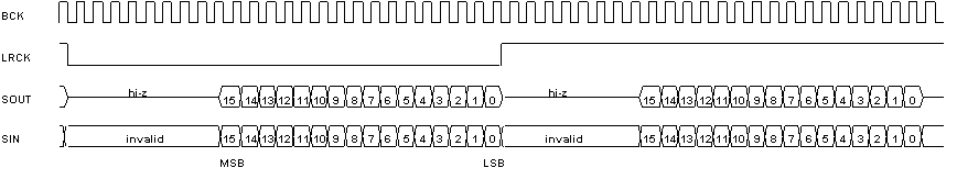
However, you need not despair if your model is not the D141, or even if your CD player isn't a Sony (everyone uses Sony chips anyways...). All CD players use a serial protocol for transmitting the digital data between components, and the serial protocol looks pretty much the same between manufacturers. With a little bit of educated guesswork and a good oscilloscope, you can find these signals (that's how I found them in the first place). The following diagram illustrates what the signals typically look like:
(sorry, it came out a bit long)
BCK is the bit clock; it runs at around 2.105 MHz, and all timing is referenced to it. BCK has a 50% duty cycle. LRCK indicates which channel is currently on the SOUT line, either the left or the right channel. The Sony computer audio databook simply specs LRCK low as being "channel 2" and LRCK high as "channel 1"; some experiments can reveal which channel maps to what speaker. LRCK has a 50% duty cycle and runs at a frequency of 44.1 kHz (hey, magic number!). I measured a frequency of 44.9 kHz, incidentally, but that is probably because my o-scope is out of calibration.
SOUT is the serial data out, and of course, SIN is the serial data in. The data is not perfectly packed between LRCK transitions because BCK may be much faster than what would be needed to pack the data just right, hence the extra time between samples is padded out with a hi-z or invalid region. There are some variations to this scheme, where the data is presented LSB to MSB, or where the data is valid at the "leading edge" of LRCK (e.g., the data happens and then the hi-z happens), but you get the idea. Looking at the signals on an o-scope, you can tell which bit position is the LSB because it is always toggling and will appear to have the hi and low portions of the trace at equal brightness; the MSB, on the other hand, toggles only when the music is very loud, and thus will tend to look rather constant.
I managed to locate these signals inside my D141 within a few minutes of probing. I first searched for the SOUT data because it is the most distnictive; the data pattern visibly shifts with the music (the CD player has to be playing when you probe for signals because in pause or in stop, the CD player stops these waveforms--probably to save power), so use your ears to help you out! Listen to some music with a good hard beat, and you can't miss the SOUT line. You can guess pretty much which chips are involved in the audio path just be looking at what they are all hooked up to. For example, the CXP508L6-005Q in my D141 was an unlikely candidate because most of the wires went to the LCD display. I figure it's probably the embedded processor which controls the whole shmeel. You can also take a tip from Sony's consistant prefix scheme...take a look in any Sony digital audio databook.
Oh, BTW, you may ask, "why don't I just look in the Sony databook?". A couple of reasons. 1) Sony is a pain to deal with when it comes to getting anything out of them, especially if you don't have a big title in a big company. 2) At the time when I did this, I am pretty sure Sony did not publish data on this chip. You probably needed an NDA (non-disclosure agreement) to get data on these babies since they are hot off the Sony drawing boards, and Sony wants to keep the technology to themselves so they can have more competative CD players than the next guy. When Sony makes the next generation of ASICs, maybe they'll release data on this chip...I doubt it though.
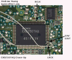
So anyways, after finding the signal, I probed each of the pins until I found the two clocks, BCK and LRCK. It wasn't too hard because I knew LRCK had to run at a magic-number speed of 44.1 kHz, and BCK had to be one of the fastest clocks and synchronous to SOUT. I'll have to hand it to Sony, their waveforms are impeccable...they look exactly like the databook waveforms, no noise, ringing, artifacts, etc. I think that the CXD2507AQ is probably a combo RF/servo control/decoder because it has a pin which generates an eye pattern and some waveforms that look pretty analog-ish and motor-control-ish to me. I mention the eye pattern pin just now because it's one of those things you look at to make sure your CD player is working right.
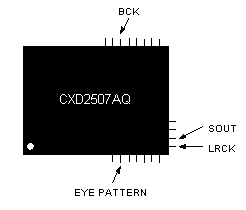
Locations of interesting pins on the CXD2507AQ
Hacking the Signals Out
Allright, enough of the exploratorium, on to the real shtuph. I'll do a step by step on how to hack the signals out to an external connector.
First, you gotta make a place for the connector to be mounted. I decided to use a standard female single-in line 0.1" spacing receptacles like the 3M 929974-01-36 (Digi-Key carries it, so does Jameco). The key thing here is to use a female socket 'cause you don't want pins sticking out of your CD player (makes it hard to put in your carrying case). I found that a spot midway on the left hand side (if the back of the CD player were facing you and the CD player is laying bottom-up) which fits a seven position connector just right. When looking for a spot, you must make sure that there are no components on the logic card that will get shorted or crushed by the connector. I cut a notch in the top half of the case with an X-acto knife to fit the connector, and hot glued it in place. Use lots of hot glue, you don't want it coming loose.
Yep, those seven holes are the connector.
Then, you gotta solder the wires in. Here's what my logic card looks like:
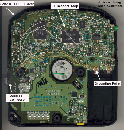
You can use this as a guide for your work, if you like. My outside connector has pins for BCK, SIN, SOUT, LRCK, and three grounds. You don't have to use all that many grounds, I'm just a phanatic for grounds.
The grounding point is the (-) terminal of the battery connector.
Soldering on the BCK and LRCK wires is pretty straightforward. Just use some wire-wrap wire, strip a bit off the end, maybe put a drop o' solder on it, and tack it onto the BCK and LRCK pins. If you look at the figure below, you can see how I used the chip as strain reliefs for the wires.
BCLK should be BCK, oops. Note how the BCK wire is fed back under the chip for strain relief.
The tricky part is soldering on the SIN/SOUT wires. The following diagram illustrates the final configuration:
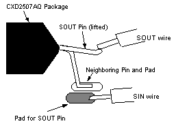
Diagram of SIN/SOUT hack
You have to do some kinda nasty hack like this because SIN is the SOUT wire in a CD player, e.g., to get both input and output you need to break the connection somewhere. You could always cut the trace on the board and just tack solder SOUT to the CXD2507AQ and tack solder SIN to the corresponding pin on the DAC, but space is tight on these boards and it is my personal preference to avoid cutting traces in situations like this (cutting traces is too permanent).
I did this by first carefully lifting the SOUT pin from the pad using a fine-tip iron and some wire hooked around the pin to provide the lifting force. Take care not to lift the pin too high; otherwise, you may break it off of the package. I then cleaned up the pad a bit by warming it. Finally, I very carefully soldered on the wires. It is important not to make a solder bridge between the top wire and the bottom wire.
Be careful where you route your wires; make sure you can close the CD player when you are done, otherwise you may have to redo some connections. The following diagram shows how I routed my wires through a large hole in the logic card.
Hey, now your done. You've got digital bits coming off the side of your CD player.
Using the Signals
OK, a few notes on useage.
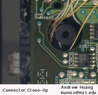
First, in order to make your CD player useable for testing you need to make a shunt to short SIN and SOUT. Installing the shunt on the external connector allows your CD player to function as it did before you did these modifications. You can kinda see the gray shunt I built in the photo above labelled "connector close-up". Make sure your shunt is sealed and small; that way when you're not using your CD player as part of some other system you can still carry it around like you used to.
Second, the signals coming out have 3V logic levels. That's right, logic low is around 0V and logic high is around 3V. They also have absolutely no drive capacity, so any capacitance will degrade signal quality. Using long ribbon cable will cause excessive crosstalk due to capacitive coupling. I recommend keeping the ribbon cable short (less than 15 cm) if possible.
I recommend using plain old CMOS 3.3V logic for the direct interface to the CD player. The first thing the signals should encounter is a buffer to boost the signal power and to protect the internal logic. Use 3.3V to 5V interface chips if you need to; you can do this with National Semiconductor's VHC series of chips for logic level conversion. You must employ some form of logic conversion for the SIN line because you can force the DAC into SCR latch-up if your outputs aren't limited to 3V. VHC series of chips have specially protected inputs so they can run with 3V supplies, for example, and take inputs with levels as high as 7V without going into latch-up.
If you don't have any logic level converters on hand, and you just want to use the outputs (BCK, LRCK, SOUT), you can feed them into standard 74ALS or similar logic if you provide 10k pull-ups to +5V to increase signal drive. This is a gross hack and it could damage your CD player if used for extended periods of time! Without these pullups, signals are too weak to drive the bases of TTL logic and capacitive effects dominate. The result is dogmeat for signals.
A cheap and dirty way to build a serial in parallel out shift register is to use a device similar to the 74ALS574 octal latch in the following manner: connect the Q[n] bit to the D[n+1] bit, eg, Q[0] goes to D[1]. D[0] is connected to SOUT. You will need to use two '574s in series to get the full 16 bits (e.g., Q[7] of the first '574 connected to D[0] of the second '574). Clock the registers with BCK or'd with LRCK, so that they are enabled only when channel 1 data is available (or NOR them if you want channel 2). Voila! You've got 16-bits in parallel, demuxed by channel, and data availability is indicated by LRCK.
Well, that's all I'm going to write for now. If you have comments or would like to share your experiences, please mail me.
Thanks to Scott Stephens who sent me pointers to a couple of web pages that discuss different digital audio transmission formats: SPDIF (1) and SPDIF (2).
Created 9/15/96 4:18 AM PST by Andrew Huang (bunnie@mit.edu)
Last modified 9/15/96 4:18 AM PST by Andrew Huang (bunnie@mit.edu)
This page was created using Netscape Navigator 3.0 Gold
(thank you Netscape! Mozilla rules!)