PRELIMINARY
Field Programmable Clock (FPC)
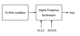
The Field Programmable Clock (FPC) features a digital frequency synthesizer PLL that is user programmable. Programming occurs via a two-wire serial interface consisting of one clock and one data wire. The PLL uses a 10 MHz crystal oscillator as a reference frequency source. The simple two-wire programming interface makes the FPC ideal for use with FPGAs where user pin count budgets often cannot afford a parallel programming interface.
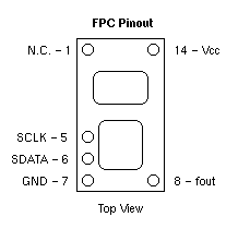
The FPC's pinout is backward-compatible with the industry standard 14-pin DIP oscillator pinout; one can plug a fixed frequency oscillator into an FPC socket once a design is mature and the operating frequency is set.
Upon power up, the FPC will output a 10 MHz clock until configured by the host. A typical FPC application would integrate an FPC programming state machine into the user's design. This state machine is activated after FPGA configuration; the 10 MHz default frequency allows the FPGA-FPC system to bootstrap itself into the desired operating frequency. The PLL can be configured in a manner which provides a glitch-free transition between the default frequency and the programmed frequency.
It is important that proper decoupling is provided across the power feed into the FPC, as PLL stability can be affected by power line noise. It is also important that Vcc have a clean, monotonic rise of less than 5 ms to spec upon power up in order to prevent the PLL from locking up.
Please see the companion data sheet, Cypress Semiconductor ICD2053B Programmable Clock Generator, Cypress document #38-00412, for further information about programming the FPC. The FPC has the same programming interface as the ICD2053B. Cypress offers a program, BITCALC, which can assist users in calculating PLL parameters.
Operating Conditions
|
Parameter |
Description |
Min. |
Max |
Unit |
| Vcc | Supply Voltage |
4.5 |
5.5 |
V |
| Ta | Ambient Operating Temperature |
0 |
70 |
C |
Electrical Characteristics
|
Parameter |
Description |
Min. |
Max. |
Unit |
| Voh | Output High Voltage |
2.4 |
V |
|
| Vol | Output Low Voltage |
0.4 |
V |
|
| Voh | Input High Voltage |
2.0 |
V |
|
| Vol | Input Low Voltage |
0.8 |
V |
|
| Iih | Input High Current |
250 |
uA |
|
| Iil | Input Low Current |
-250 |
uA |
|
| Cin | Input Capacitance |
10 |
pF |
|
| Icc | Power Supply Current |
130 |
mA |
Switching Characteristics
|
Parameter |
Name |
Description |
Min. |
Max. |
Unit |
| T | Output Period | fout period (frequency) |
10 |
2560 |
ns |
| D | Duty cycle | Duty cycle of fout measured at TTL thresholds |
40% |
60% |
|
| Tr | Rise Time | Rise time for fout into a 25 pF load, TTL levels |
3 |
ns |
|
| Tf | Fall Time | Fall time for fout into a 25 pF load, TTL levels |
3 |
ns |
|
| Tsclk | SCLK period | Minimum cycle time for SCLK |
200 |
ns |
|
| Ts | Serial Data Setup | Time required for the data to be valid prior to the rising edge of SCLK |
15 |
ns |
|
| Th | Serial Data Hold | Time required for the data to remain valid after the rising edge of SCLK |
0 |
ns |
|
| Tlock | VCO Lock Time | Time for VCO to lock onto new frequency within 0.1% |
10 |
ms |
|
| Tstart | Startup Time | Time for fout to stabilize after Vcc is stable |
25 |
ms |
|
| Ttr | Transition from reference to programmed frequency | Time for fout to go high after release of internal mux |
0 |
125 |
ns |
Mechanical Characteristics
 Document
number 1000-904-001-X0
Document
number 1000-904-001-X0
FPC is Part Number 1000-004-001-X0
Date: 12/4/97
Copyright (c) 1997 Andrew Huang and
Xtreme Ideas Technology Development
Specifications subject to change without notice.
This data sheet is preliminary.
Data and text in this document are derived from the Cypress Semiconductor ICD2053B data sheet and the Connor-Winfield HSM91 data sheet.
The Xtreme Ideas logo is a trademark of Xtreme
Ideas Technology Development.
Xtreme Ideas Technology Development assumes no responsibility
for the use of any circuitry other than circuitry embodied in an Xtreme
Ideas Technology Development product. Nor does it convey or imply any license
under patent or other rights. Xtreme Ideas Technology Development does
not authorize its products for use as critical components in life-support
systems where a malfunction or failure of the product may reasonably be
expected to result in significant injury to the user. The inclusion of
Xtreme Ideas Technology Developmeent products in life-support systems applications
implies that the manufacturer assumes all risk of such use and in so doing
indemnifies Xtreme Ideas Technology Development against all damages.