Optical Arbitrary Waveform Generator
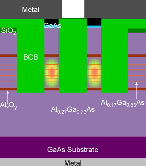
Figure 1) Cross-section illustration of a waveguide modulator structure.
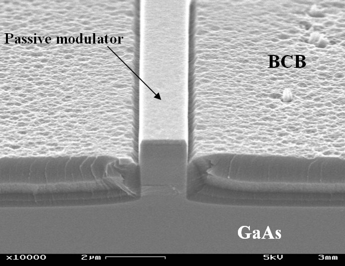
Figure 2) Facet view of the passive waveguide planarized with BCB. The waveguide leads into and out of the powered Mach-Zehnder interferometers.
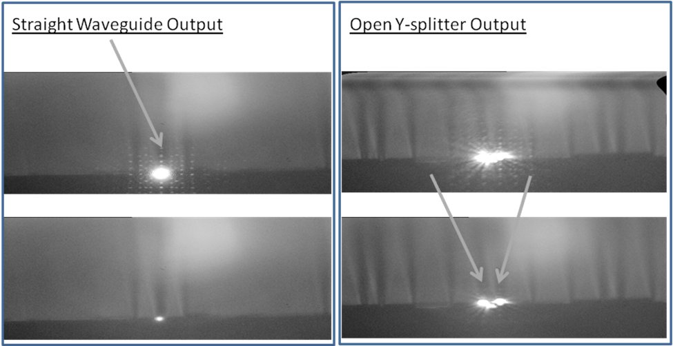
Figure 3) Facet views of successful optical transmission at the outputs of a straight waveguide (left) as well as a Y-splitter (right).
Optical signal modulation is a cornerstone of communication systems, allowing the transfer of information from the electrical domain to the optical domain. By transforming an incoming pulsed optical source into an optical frequency comb using arrayed waveguide gratings and employing both phase and amplitude modulation using Mach-Zehnder interferometers, an arbitrary optical waveform is constructed following the recombination of the frequency comb.
Electro-optic modulation of frequency combs that are centered at a wavelength of 800nm requires the use of GaAs-based materials that are transparent to light of that wavelength. A structure (shown schematically in Figure 1) consisting of alternating high- and low-index AlGaAs materials, low-index AlGaAs cladding layers, and AlAs (that can be transformed to AlxOy with oxidation methods) layers has been grown by molecular beam epitaxy and processed into Mach-Zehnder interferometers that consist of 2-micron-wide waveguides and active modulators. To create the largest mode possible and to minimize the coupling loss, the index contrast between the waveguiding layers and the cladding layers is minimized through the use of a dilute waveguide structure in which thin layers of high-index material are embedded in a low-index material. The resulting layered structure has an effective index slightly higher than the low-index material and is determined by the layer thicknesses as well as the refractive index of the two materials that comprise the dilute waveguide. The oxidized AlAs layers strongly confine the optical mode to the middle of the structure and are expected to allow the device to withstand higher operating voltages without concern about breakdown or carrier loss.
Fabrication of the electro-optic modulator employs a self-aligned photolithography and etching process to ensure successful optical transfer between the passive and powered waveguide regions that are defined in separate steps. The fabrication process utilizes an inductively-coupled plasma reactive ion etch (ICP-RIE) step for the definition of all waveguides to minimize the optical losses in the system. Photolithography process developments that are used in conjunction with anisotropic ICP-RIE etches, allow for consistency in the fabrication of ridge waveguides with straight sidewalls and minimal roughness. Passive measurements of fabricated structures, as seen in Figure 2, yield an optical insertion loss of 9.6db/cm using the optimized ICP-RIE processes. Successful 3dB power splitting in Y-splitters has also been observed, as shown in Figure 3.
