Department
of Chemical Engineering
Room 66-217
Massachusetts Institute of Technology
77 Massachusetts Avenue
Cambridge, MA 02139-4307 USA
Telephone (617) 253-6586
Fax: (617) 258-8840
Email: srasgon@mit.edu

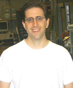
Stacy A. Rasgon
Graduate Research Assistant
A.A., Liberal Arts, Los Angeles Pierce College, 1997B.S., Chemical Engineering, UCLA, 1999
Research Interests
Origin, Evolution, and Control of Sidewall Line Edge Roughness Transfer During Plasma Etching
The next generation of microelectronic devices will require etching of polysilicon taken down to the nanometer range and smaller.For the patterning of sub 100 nm features, a clear understanding of the origin and control of line edge roughness (LER) is extremely desirable, both from a fundamental as well as a manufacturing perspective. 'Line edge roughness' has typically been studied in the lithography community, and LER studies have focused on the analysis of top-down scanning electron microscopy (SEM) micrographs of post-developed photoresist lines. However, the effect of plasma etch on sidewall roughness has been overlooked. Plasma etching processes often roughen the feature sidewalls, leading to the formation of anisotropic striations. From a manufacturing perspective, it is the post-etch sidewall roughness, rather than the post-lithography LER, which will ultimately limit device performance.
My research focuses on the observation of sidewall roughness via a novel atomic force microscope (AFM) technique. The resulting images allow the extraction of quantitative information on sidewall roughness and spatial frequency as a function of depth, and the observation of the transfer of roughness through multiple layers simultaneously, thus vividly highlighting the structure of the post-etch sidewall. My work involves using this and other techniques to systematically study the mechanism of roughenss transfer to underlayers during processing, while examining the roles of different etching steps (anti-reflection coating (ARC)open, hardmask open, substrate etch, etc.) on the roughness propagation. I also have examined the interaction of the etching process with the photoresist material type (for example, different etching chemistries interacting with fluorinated resists), and examined the roughening of low - k dielectric flims in fluorocarbon plasma chemistries. Finally, I am undertaking what we believe to be the first fundamental study of sidwall roughness development through the use of a newly-constructed realistic plasma beam apparatus, which enables a sample to be impinged by a directional ion flux with independent control of the ion bombardment energy, ion impingement angle, and plasma chemistry.
Personal Interests
My technical interests include plasma processing and surface science. I also enjoy mechanical design (a useful skill in this lab), and have become a rather competent machinist during my tenure here at MIT. Outside of technology, my interests are wide-reaching. I play the trombone, sail, and read voraciously. I am interested in business, finance, and real estate, and own a condo in East Cambridge, where I serve on the board of trustees.