Silicon Solar Cells
Home / Research / Energy Conversion / Solar Cells / Silicon
Amorphous Silicon
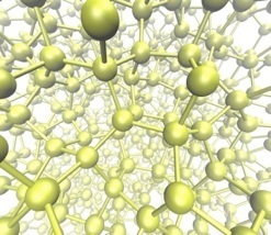
While amorphous silicon(a-Si) is made of the same silicon atoms with the same four-fold coordination as crystalline silicon(c-Si), the bond network is disordered, which makes the electronic structure very different. C-Si does not absorb light very well, but is a good conductor of charge carriers, but the disorder in a-Si reverses these properties.
The high light absorption of a-Si allows us to make ultra-thin solar cells, with the entire package around one micrometer thick, as compared to five hundred micrometers for traditional c-Si cells. One can purchase them today for rooftop installation. However, the efficiency is lower than c-Si cells, so they must be larger to provide the same amount of power. A-Si also suffers from the long-standing Staebler-Wronski effect (SWE), in which the efficiency drops as the cell is exposed to light. Current research indicates that the SWE is due to some microscopic structural transition, although there is still no consensus on what that transition is.
Thus microscopic structure is important both for the Staebler-Wronski effect and for general device design, since different networks of silicon behave differently electronically. We employ a combination of methods to study a-Si networks, from very accurate and expensive electronic structure calculations (quantum Monte Carlo) to density functional theory to simple rate equations. For more information see L.K. Wagner and J.C. Grossman, PRL 101, 265501 (2008). At present we are working on new approaches for mitigating the SWE based on these results.


Tapered Nanowires
Nanowires are observed experimentally to be tapered rather than straight-edged, with diameters shrinking by as much as 1 nm per 10 nm of vertical growth, depending on the synthesis techniques and conditions. Yet, previous theoretical work to understand the electronic, optical, a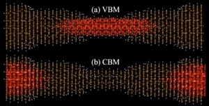 nd structural properties of nanowires have assumed a straight-edge geometry. In this study, we find that tapering has a profound effect on the optical and electronic properties of silicon nanowires by ab initio calculations. Axially-dependent electronic structure attributes are predicted with unoccupied eigenstates substantially more sensitive to diameter than occupied ones. Remarkably, the states corresponding to the highest occupied and the lowest unoccupied bands are spatially separated along the wire axis, which can be explained by the interplay between a strong variation in quantum confinement strength with diameter and the tapering-induced interface states.
We are investigating the possible usages of this unique property in electronic and optical devices. One example of a way to take advantage of this unique effect would be in a solar cell, where thermalization and internal electric fields could separate spatially the electron and hole into different ends of the tapered nanowire. Thus the charge separation can be driven in a pure material without doping. For more information see Z. Wu, J.B. Neaton, and J. C. Grossman, Phys. Rev. Lett. 100, 246804 (2008).


Charge Separation by Controlling Nanoscale Morphology
In this work we explore new ways of separating electrons and holes in silicon solar cells without doping. In a typical p-n junction device doping is required to create an electric field that separates the charges. By taking advantage of unique properties of the dependence of energy levels on nanoscale morphology, we have identified several different approaches that could be used to bring electrons and holes to opposite sides of a pure, undoped material. This could lead to major cost savings as well as the possibility of using lower-grade material. More details on this work will be presented here soon.

Massachusetts Institute of Technology, 77 Massachusetts Avenue, Cambridge MA 02139-4307
