| Kastner Group | Home | People | Research Projects | Papers and Publications | Lab Tour | Posters |
|
|
|
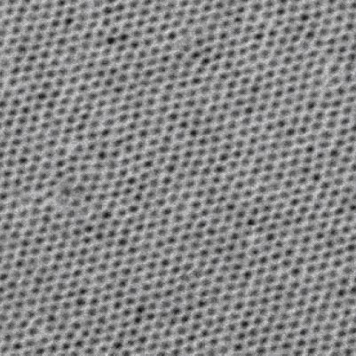
Electronic Transport Properties of PbSe Nanocrystal ArraysWe study electron transport in arrays of PbSe nanocrystals (NC) in collaboration with the Bawendi Group in the Department of Chemistry. When the radius of a semiconductor nanocrystallite is smaller than the bulk exciton Bohr radius, the electron and hole experience quantum confinement in three dimensions. For this reason, semiconductor NCs can be thought of as quantum dots or artificial atoms. By controlled chemical synthesis, we can tune the energy levels of individual NCs as well as the electronic coupling between NCs in an array. To study the electron transport properties, we fabricate an inverted field-effect transistor (FET) with the NC array serving as the transport channel. We are able to measure the current as a function of source-drain voltage and to modulate the charge density in the array with the back gate (Charge Transport in Arrays of PbSe Nanocrystals).
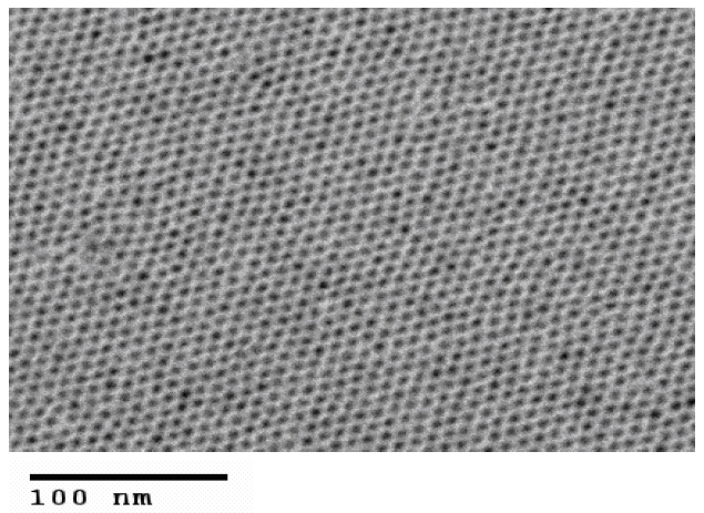
TEM image of a highly ordered monolayer of PbSe quantum dots.
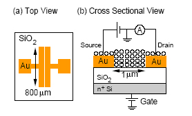
Schematic of the inverted FET and the circuit used in the experiments. We are presently studying the transport properties of a NC array through charge sensing rather than measurement of current as in the inverted FET. The goal is to fabricate a device with multiple charge sensors positioned adjacent to a small array of NCs. Through triangulation of the charge sensors, one can determine the position of an electron moving through the array. Thus, one can study the dynamics of tunneling between localized states and the distribution of trapped charge. A deeper understanding of electron tunneling between localized states is important for improving the efficiency of solar cells. Trapping of charge in localized states in amorphous semiconductors limits the efficiency of solar energy conversion. Furthermore, novel solar cells made from nanostructures, such as semiconductor nanocrystals, rely on tunneling between localized states. |
| Home
| People
| Research Projects
| Papers and
Publications
| Lab
Tour
| Posters
|
||