A Smooth Optical Superlens
|
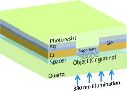
We utilize a unique approach to grow ultrasmooth silver films characterized by much smaller root mean square (RMS) surface roughness. An intermediate ultrathin Ge layer ( ~1nm) is introduced before depositing Ag. Utilizing Ag–Ge surface interactions, smooth superlens down to 15 nm Ag thickness was fabricated. Roughness measurements of thin silver films (15 nm) deposited with and without Ge layer (1 nm) were performed using atomic force microscopy (AFM) and x-ray reflectivity techniques. These measurements indicate drastic improvement in Ag surface morphology with roughness below 0.8 nm with introduction of Ge layer. It is postulated that Ge acts as a wetting layer for Ag and helps a layer by layer growth. A detailed study of the growth of Ag on Ge has been described elsewhere.9 Some earlier works have indicated that thin and smooth Ag films can also be prepared epitaxially with metal oxides such as magnesium oxide and nickel oxide. The configuration of the smooth silver superlens is illustrated in left Figure. An array of chrome (Cr) gratings 40 nm thick with 30 nm half-pitch, which serve as the object, was patterned using a nanoimprint process developed by Hewlett-Packard Laboratory.
Figure (Left)
Schematic
drawing of a smooth silver superlens with embedded 30 nm chrome gratings
on a quartz window, operating at 380 nm wavelength. To prepare the
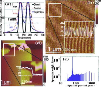
smooth superlens, a thin germanium layer is seeded. (Right) (a) Computed
image modulation with superlens FWHM = 37 nm (blue dashed curve) and
without superlens FWHM = 113 nm (red dotted curve). (b) Subdiffraction
optical imaging with superlens: AFM of developed photoresist with zoom
in panel showing section analysis. (c) Fourier analysis of the developed
image grating. (d) Near-field optical imaging without superlens.
Right Fig. b
shows the image of the Cr grating area recorded on the photoresist layer
after exposure and development. It is evident from section analysis of
the recorded image (zoom in panel) that with careful control of surface
morphology, the recorded image has ~6nm height modulations. The
Fourier-transformed spectrum shows clear peaks up to third harmonic of
the 60 nm pitch Cr gratings recorded on the resist layer [right Fig. c].
In a control experiment, when the Ag–Ge layers are replaced by equally
thick spacer layer, we observe that only a portion of grating area is
developed [right Fig. d]. Moreover, the developed wires are much thicker
(~47nm) and the poor contrast suggests loss of
resolution as predicted by the PSF calculation. This confirms that
near-field imaging alone without evanescent enhancement is not capable
of resolving high-frequency spatial features (~λ/12) located just 27nm(
= λ/14) away from the surface.
|