Photovoltaic Manufacturing Lab
Mission Statement
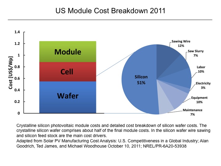
Photovoltaic cells produce emission-free electricity without moving parts, large capital investment, or active cooling. Modular photovoltaic systems can be installed in remote areas to provide off-grid communities with electricity. Unfortunately, crystalline silicon photovoltaics (c-Si PV) are presently not a cost-competitive technology for grid-electricity generation. The most expensive component of a photovoltaic module is the silicon wafer. Our objective is to develop a kerfless silicon wafer manufacturing technology that will substantially reduce the production costs of high quality multicrystalline silicon wafers.
Project Overview
It is well established that photovoltaics can achieve grid-parity economics if the cost of the module is below $1/Wp (Wp is the peak wattage attainable by a solar cell given AM1.5G insolation). Silicon wafers for solar cells are traditionally made by a multiple-step, consumable-intensive process where large silicon ingots are cast and then subsequently wire-sawn into individual wafers. The single-use steel wire and grinding slurry consumed in this stage is costly, but more importantly, manufacturing wafers via wire-sawing wastes over half of the silicon feedstock in the form of kerf (width of each cut). A kerfless wafer manufacturing process that can yield high quality silicon wafers would have resounding impact on the economics of photovoltaics.
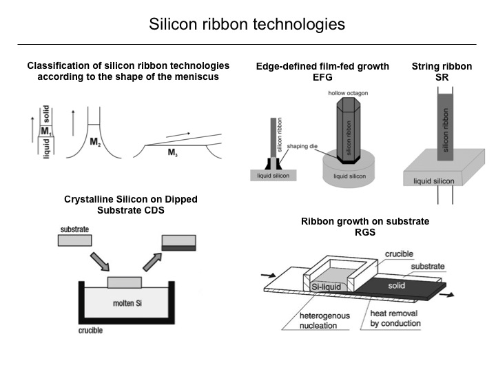
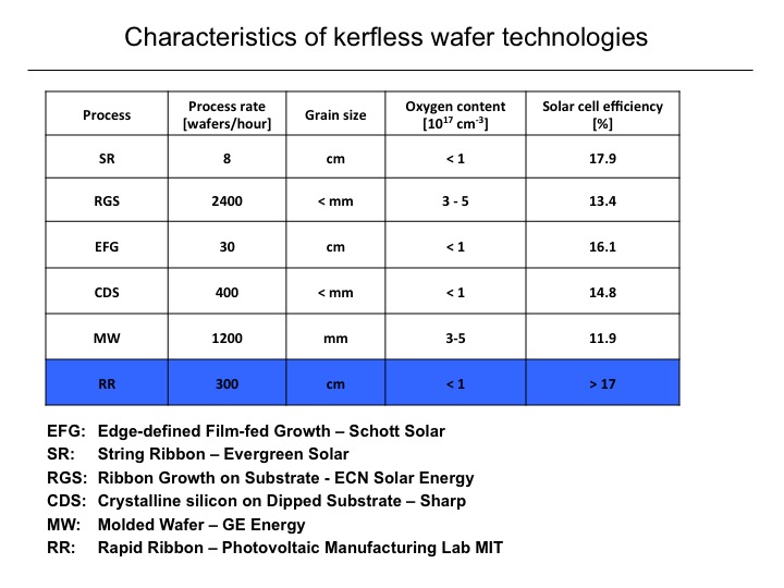
To date, demonstrated kerfless technologies have suffered from either low production rates, low material quality, or were not economically feasible. Our objective is to substantially reduce the manufacturing cost of crystalline silicon solar cells by developing a novel kerfless wafer technology that produces high quality wafers at accelerated process rates. If successful, our proposed process would dramatically impact the multicrystalline silicon wafer industry which has exponentially increased to a $4 billion market over the last decade [Renewable Energy Corporation, Fourth Quarter 2011 report]. Furthermore, the cost reductions from our approach would make c-Si photovoltaics an economic alternative to conventional grid power sources.
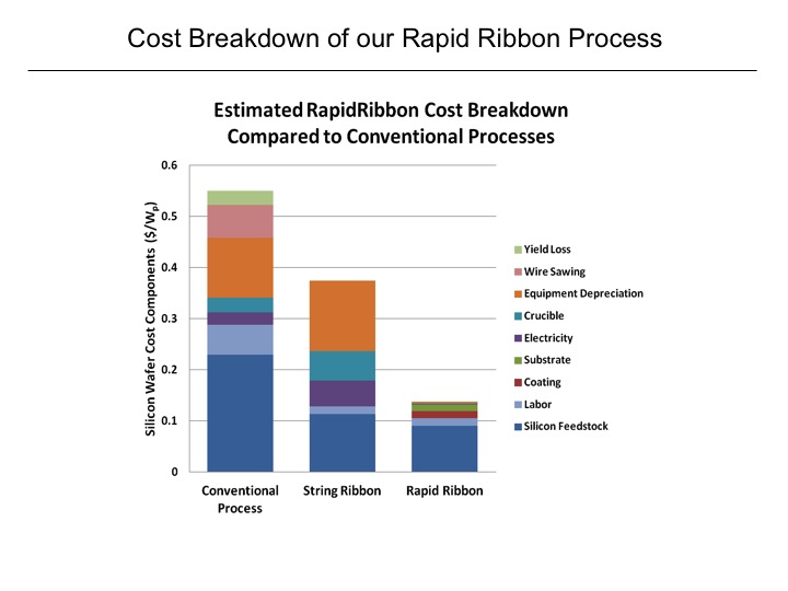
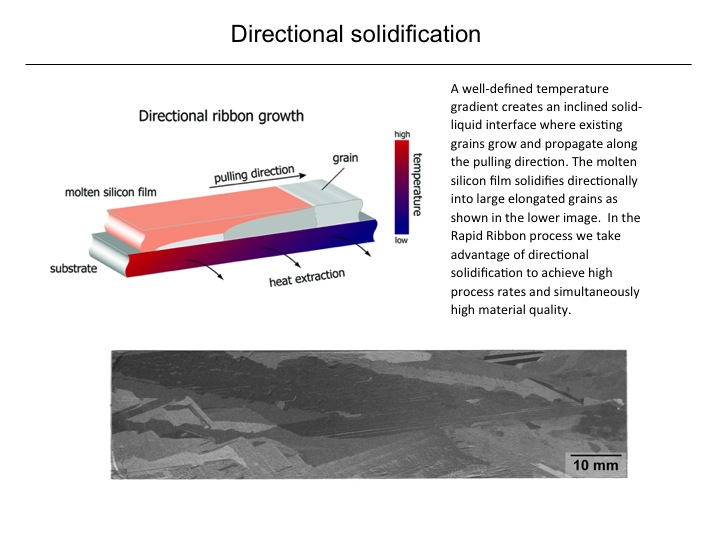
Unlike past approaches, our proposed silicon wafer manufacturing process, ‘Rapid Ribbon’, grows a ribbon via a carefully tailored thermal profile. Prior work developed at MIT has demonstrated that it is possible to create and maintain a well-defined inclined solidification interface in a thin film of molten silicon. An inclined solidification interface allows a silicon film to be directionally solidified at high growth rates without compromising the material quality. Our novel approach will form net shaped wafers with superior microstructure by isolating a thin liquid film from a molten bath of silicon at process rates of over 300 wafers/hour.
Built with Twitter Bootstrap
Ana Ruelas 2012