Writing With Atoms.
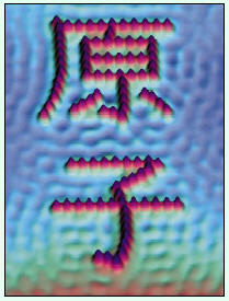
Written literally with atoms, the Japanese Kanji above—each just a few nanometers across—means "atom."Nanotechnology – Shaping the World Atom by Atom (NSTC report). I. Amato. 1999. Brochure for the public (this report); available on the Web:
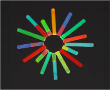
http://itri.loyola.edu/nano/Polymer rods embedded with cadmium selenide nanocrystals, fluorescing at various wavelengths (M. Bawendi et al.; photograph by Felice Frankel — copyright reserved). This photograph suggests the broad societal implications of nanoscience and nanotechnology.
From: www.nano.gov: Societal Implications of Nanoscience and Nanotechnology, NSET Workshop Report,
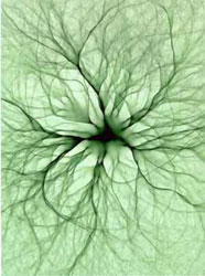
Edited by Mihail C. Roco and William Sims Bainbridge, National Science FoundationScanned microscope images of
electron flow away from a quantum
point contact.
Robert Westervelt, Harvard University