DIY Scanning Tunnelling Microscope
My STM project from spring-fall 2012. It was an exciting few months of ordering parts from obscure manufacturers, doing tons of Solidworks revisions, and attempting to simulate a tunneling junction in SPICE, but eventually I ended up with a working STM.
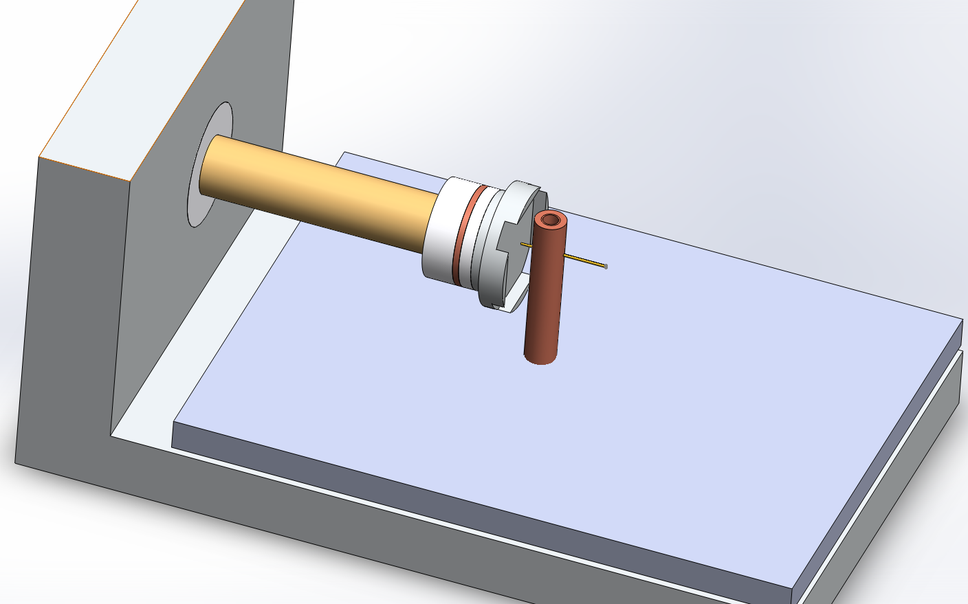
This is the final solidworks model of the hardware. It has exact models of the piezos I bought, at well as shape refinements intended to ease the machining process. I also was forced to use a wire to carry the probe current, as stick-slip motion would be very difficult to achieve with the added friction of a spring-loaded contact. I also made the design more modular.
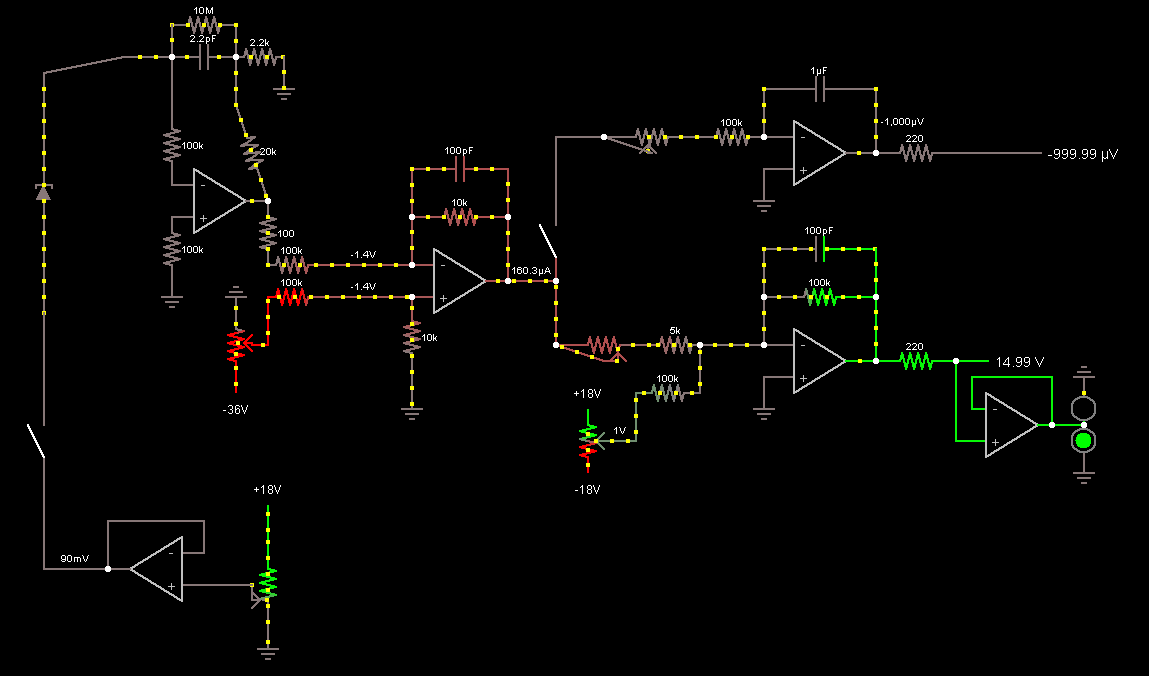
A circuit I designed to keep the STM probe head within quantum tunneling distance of the sample. A very sensitive feedback circuit responds to the voltage across the tunneling junction.
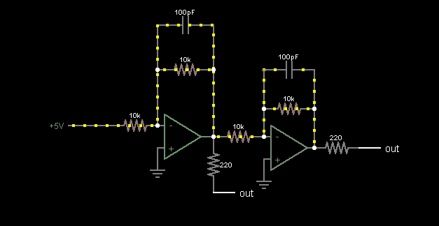
A circuit to control the XY movement of the stage to raster the probe across the sample. Two of these, one for each axis, were used and controlled by an arduino. I chose an x-y piezo tube from Boston Piezo-Optics.
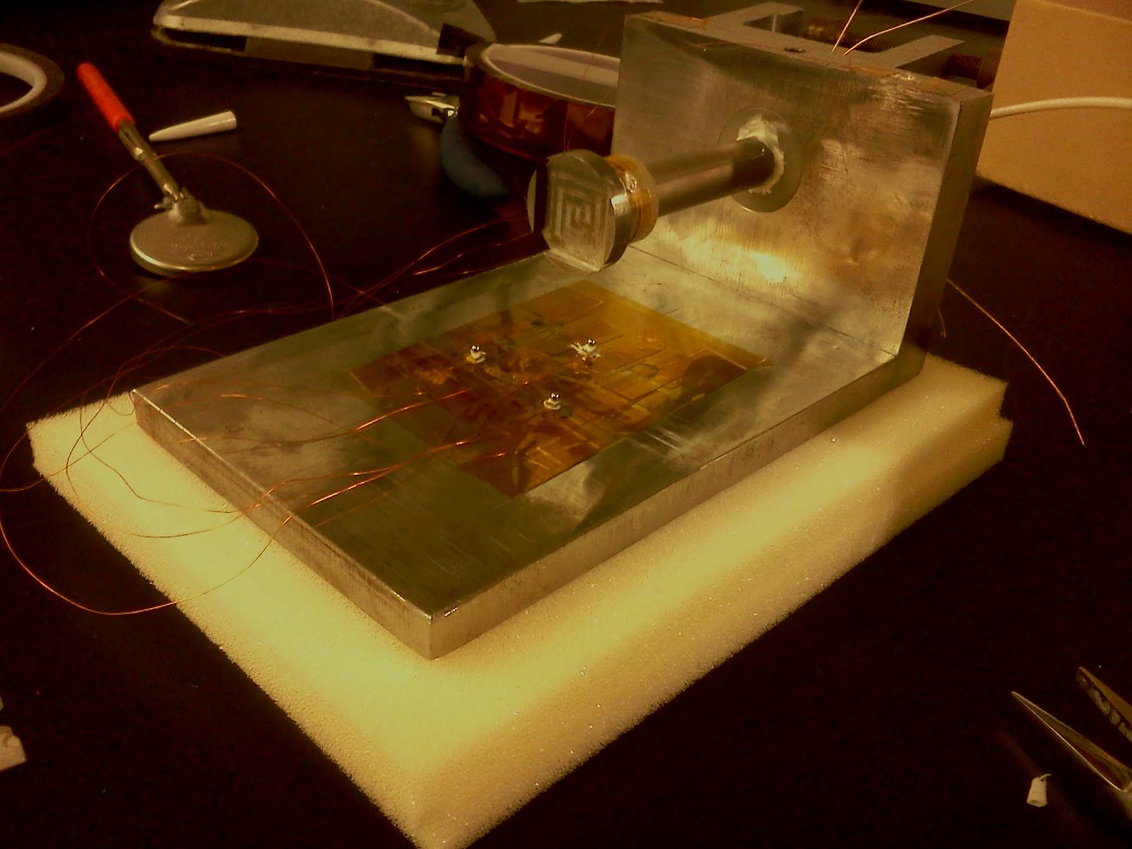
The STM base stage consisting of a piezo tube to control the x/y position of the probe, and three shear piezos to create a stick-slip motion for the probe approach. A saw wave was applied to the three shear piezos at the bottom; they would carry the probe platform in one direction relatively slowly during the slope, and then would rapidly be jerked back leaving the probe in the same place due to inertia. This allows for incremental movement on the order of a few nanometers, in order to initially bring the probe close enough for tunneling to start. The voltage amplitude of the saw wave required for this was high enough that I had to use a computer-controlled voltage source at the California NanoSystems Institute.
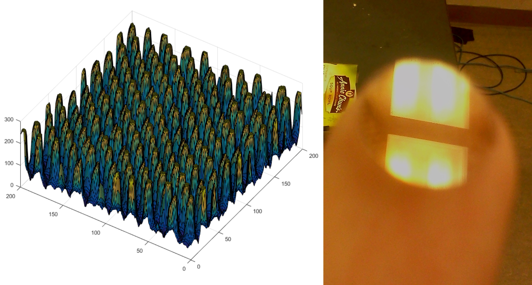
A 22x22 Angstrom raster of a gold calibration sample, shown on a fingertip for size. Once a tunneling voltage was locked in and the raster was performed, the minimum and maximum z-values were mapped from 0-255 for easy visualization.
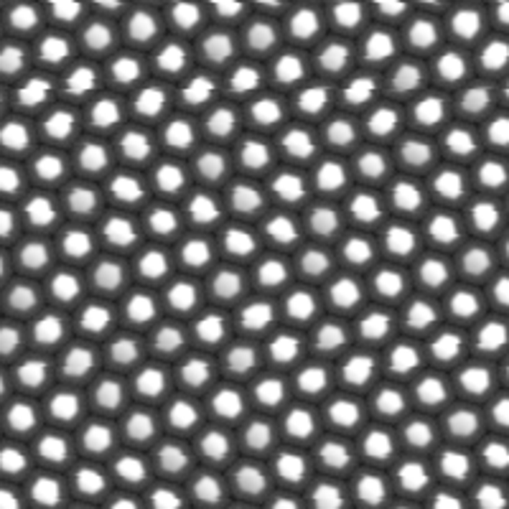
An image of the gold atoms, with an XY resolution of 200 samples.