Ultra Low-power Analog VLSI Design (6.376)
Design of ultra-low power ECG Amplifier
 In this course, George Kakuru and I designed and laid out a low-power, low noise and high gain EKG amplifier in 0.18um standard CMOS technology. This amplifier can be used as part of a wireless EKG monitoring system powered by rectified radio-frequency energy or other forms of energy harvesting like body vibration and body heat. The EKG signal was collected by a pair of electrodes connected to the human body at two locations ( i.e. left arm and right arm). The instrumentation amplifier (IA) topology was used for this design for its high gain, high input impedance and high CMRR. Unlike the traditional IA, we used capacitors to set the high frequency gains and adaptive MOS elements to set the low frequency gains which helped reduce mismatch, noise and power consumption of the EKG amplifier. The basic amplifiers
used in this topology were operational transconductance amplifiers (OTAs) where PMOS input transistors were operated
in subthreshold region to improve 1/f noise efficiency, and the mirror transistors operated in strong inversion to minimize
the thermal noise. Two major challenges were presented by this project; common-mode interfering 60-Hz picked up the
electrodes and mismatch between components during the simulation of the extracted chip. The former one was mitigated
by adding a third electrode in combination with a common-mode feedback amplifier, a super buffer and a Gm-C notch
filter to yield better performances and attenuate the 60-Hz noise. The latter one was minimized by implementing a
common-centroid layout technique which greatly helped reduce the mismatch between the gain setting capacitors. The power consumption, the input-referred noise, and the CMRR were 8uW, 7.5uVrms and 118dB respectively. The final chip area was estimated to be around 500umx500um. This bioelectronics class was one of the most rewarding classes I took at MIT in terms of both the difficulty of the lecture materials and complexity of the final project. Through the great lectures of Prof. Rahul Sarpeshkar and this project, I learned a great deal about the challenges presented in designing ultra-low power circuits for various applications particularly in energy harvesting circuits and implantable electronic devices. I also learned that a great part of the design process in custom mixed-signal circuits that include transistors requires a great deal of intuition given the variation of transistors across operating conditions. Here is the link to the final presentation.
In this course, George Kakuru and I designed and laid out a low-power, low noise and high gain EKG amplifier in 0.18um standard CMOS technology. This amplifier can be used as part of a wireless EKG monitoring system powered by rectified radio-frequency energy or other forms of energy harvesting like body vibration and body heat. The EKG signal was collected by a pair of electrodes connected to the human body at two locations ( i.e. left arm and right arm). The instrumentation amplifier (IA) topology was used for this design for its high gain, high input impedance and high CMRR. Unlike the traditional IA, we used capacitors to set the high frequency gains and adaptive MOS elements to set the low frequency gains which helped reduce mismatch, noise and power consumption of the EKG amplifier. The basic amplifiers
used in this topology were operational transconductance amplifiers (OTAs) where PMOS input transistors were operated
in subthreshold region to improve 1/f noise efficiency, and the mirror transistors operated in strong inversion to minimize
the thermal noise. Two major challenges were presented by this project; common-mode interfering 60-Hz picked up the
electrodes and mismatch between components during the simulation of the extracted chip. The former one was mitigated
by adding a third electrode in combination with a common-mode feedback amplifier, a super buffer and a Gm-C notch
filter to yield better performances and attenuate the 60-Hz noise. The latter one was minimized by implementing a
common-centroid layout technique which greatly helped reduce the mismatch between the gain setting capacitors. The power consumption, the input-referred noise, and the CMRR were 8uW, 7.5uVrms and 118dB respectively. The final chip area was estimated to be around 500umx500um. This bioelectronics class was one of the most rewarding classes I took at MIT in terms of both the difficulty of the lecture materials and complexity of the final project. Through the great lectures of Prof. Rahul Sarpeshkar and this project, I learned a great deal about the challenges presented in designing ultra-low power circuits for various applications particularly in energy harvesting circuits and implantable electronic devices. I also learned that a great part of the design process in custom mixed-signal circuits that include transistors requires a great deal of intuition given the variation of transistors across operating conditions. Here is the link to the final presentation.
RF Circuits Design (6.776)
In this class, I designed a low noise amplifier (LNA) for the mid-term project and an RF Receiver Front End for the final Project.
1. Design of Low Noise Amplifier (LNA): Mid-Term Project
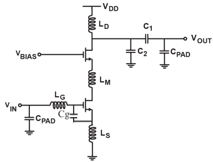 The mid-term project involved the design of high-frequency LNA for RF applications. I used the source-degenerated cascode LNA (made of the common source and the common-gate amplifiers) as the core topology. However, additional components were incorporated into this basic topology to improve the stability, S11 and the power gain. Furthermore, the devices were sized such that the noise figure(NF) is as mimimum as possible. In this design, I added a capacitor between the gate and source in the common-source stage to improve the the unity gain frequency without changing the gm of the device. A very small inductor was also incorporated between the common-source and the common-gate amplifiers to improve the stability of the LNA over a wide range of frequency. Additionally, in an effort to reduce gate resistance(Rg) and to improve the frequency response, multiple gate fingers were used. S11 of -15dB, power gain of 22dB, Noise Figure of 1.7dB over 300MHz around the center frequency and power consumption of 10mW was accomplished. The simulation for this design was performed using the 250nM IBM PDK in cadence.
2. Design of RF Receiver: Final Project
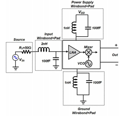 The final project in this course, involved the design of a high frequency RF receiver front-end. The receiver included the following building blocks; LNA, Voltage controlled oscillator(VCO) and a Mixer. The mid-term project LNA was modified to meet the feedthrough and instability introduced by the additional loading effect from the mixer and the VCO. I came up with a unique LNA design for this project by incorporating an additional MOSFET between the output of the source-degenrated cascode LNA and the power supply.
Power Electronics (6.334)
This is a graduate level power electronics course taught by Prof. David Perrault. In this course, I studied the design of different kinds of AC/DC and DC/DC power converters including but not limited to Buck Converters, Boost Converters, Buck Boost Converters, AC/DC Converters and the design and selection of switching devices such diodes, transistors as well as the design of inductors.
Design of a Buck-Converter
 The final project involved designing a buck converter, which converts a 22V-32V DC input voltage to a
15V DC output, under a resistive load variation from 1.5 to 4.5. A voltage-mode PI controller is designed to stabilize the averaged system under input and load variations. Detailed analysis of electrical and thermal device specifications are performed and the simulation was done in LTSpice. The worst-case efficiency of this buck converter was above 94.59%
The final project involved designing a buck converter, which converts a 22V-32V DC input voltage to a
15V DC output, under a resistive load variation from 1.5 to 4.5. A voltage-mode PI controller is designed to stabilize the averaged system under input and load variations. Detailed analysis of electrical and thermal device specifications are performed and the simulation was done in LTSpice. The worst-case efficiency of this buck converter was above 94.59%
Analog Mixed-Signal IC Design (6.775)
This course encompasses the design of a wide-range of analog and mixed-signal integrated circuits. The mid-term project for this class involved the design of an amplifier in the 60nm CMOS process technology.
Design of a 12 bit SAR ADC
Digital Systems Lab (6.111)
Audio Conference Communication System (ACCS)
 Saher Ahwal, Xianzhen Zhu and I implemented a digital conference communication system on 4 FPGA boards where one board acts as the communication coordinator and the three others act as calling stations. We succeeded in establishing calling and connecting all three callers in conference or pairs independently. We also implemented display module to show the state of the current call or connection. We were able to implement a Voicemail module that records up to 4 Voicemail messages on the ZBT RAM of the FPGA labkit. The detailed description and some of the code of the project is in the course website here
MEng Thesis
Optoelectronic Activation Function
 As part of the MIT SuperUROP research program and later my Master's thesis project, I worked with Prof. Cardinal Warde in the Photonics Systems Lab at MIT on the design and analysis of a novel optoelectronic activation function (OAF) for a Compact Optoelectronic Integrated Neural (COIN) processor. The COIN processor, a hardware prototype of artificial neural processor, implements neural networks algorithms in native optoelectronic hardware in order to perform parallel computation in a faster and more efficient manner than all-electronic or all-optical implementations. The innovation of the COIN comes from its potential to utilize the processing power of traditional electronic integrated circuits with the communication benefits of optics to provide three-dimensionally scalable architectures. The OAF is a light in-light out module which uses a combination of optical and electrical devices to perform intensity thresholding based on the magnitude of the input intensity and the thresholding value. The OAF is the core component in the COIN processor. I came up with three different circuit designs for the implementation of the OAF both in PCB and in IC level. I implemented one of the designs in a PCB as a proof-of-concept using off-the-shelf electronic components. I also simulated and laid out the remaining two designs in cadence. I optimized the overall architecture of the original COIN processor by replacing some of the bulky optical devices with electrical elements to improve the area, power efficiency and cost in order to meet the long-term goal of integrating COIN into real world systems. These systems might include facial recognition, image segmentation for medical applications, robotic guidance, and control, among others. We are preparing a journal paper on this work, to be submitted to the IEEE electronics letters in the Spring of 2016. This project has taught me important skills including researching, reading, and analyzing the literature around a specific research problem.
MIT $100K Competition
Rhyno Bluetooth Ring
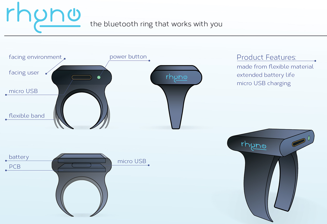 MIT didn't only teach me how to be innovative engineer but also challenged me to be entrepreneurial and collaborative. In reference to this, Rhyno, a startup idea in wearable technology that was envisioned by my college roommate and myself, was selected as a semi-finalist in one of the most prestigious MIT $100K entrepreneurship competition. Rhyno is a Bluetooth-enabled, compact, seamless and affordable ring that is empowered by a precise hand gesture recognition algorithm to detect complex hand motions with the aid of a 9-axis IMU, and a Microcontroller. Rhyno has a wide variety of uses in smart-home, assistive technology and gaming applications. Video