


Next: Netlist the Design
Up: Example
Previous: Example
Contents
Figure 1 shows the
schematic of a simple switched capacitor circuit.
Figure 1:
Simple Switched Capacitor Circuit
|
|
Note that some switches, S1 and S3 for example, are controlled by CLK1
while others, S2 and S4 for example, are controlled by the complement
of CLK1 (#CLK1).
Figure 2 shows the definition of a clock and the master
clock. Here we define a master clock period (mcp) of 1.0  s in
the timing block.
s in
the timing block.
Figure 2:
SWITCAP Clock Definition Schematic
|
|
In the clock definition symbol, we define a clock called CLK1 that has
a period equal to 1 master clock period (mcp). The phase of CLK1
turning on switches is 0 and the phase of CLK1 turning off switches is
3/8 mcp. Additional clock phases can be defined by creating more
instances of the clock definition symbol.
Figure 3 shows an instantiation of the title block
symbol which will cause ``my title'' to be used in the TITLE line in
the SWITCAP netlist.
Figure 3 also shows an instantiation of an analysis
block which directs the netlister to include the contents of the file
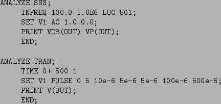
test.ana in the output netlist. Figure 4 shows
the contents of the test.ana file.
Figure 3:
SWITCAP Analysis Definition Schematic
|
|
Figure 4:
SWITCAP Analysis File, test.ana
 |
Next: Netlist the Design
Up: Example
Previous: Example
Contents
Stuart Brorson
2005-03-15