| | Introduction to TEM Waves |
|---|
| 13.1.1* | With a short at y = 0, it is possible to find the fields for
Example 13.1.1 by recognizing at the outset that standing wave
solutions meeting the homogeneous boundary condition of (12) are of
the form Ex = Re A sin ( y) exp (j y) exp (j t). t).
Hz and the dispersion equation (relation between  and and
 ). ).
| (a) | Use (13.1.2) and (13.1.3) to determine the associated
|
| (b) | Now use the boundary condition at y = -b to show that the
fields are as given by (13.1.16) and (13.1.17).
|
|
| 13.1.2* | Take the approach outlined in Prob. 13.1.1 for finding the fields
[(13.1.28) and (13.1.29)] in Example 13.1.2.
|
| 13.1.3 | Assume that  o is real and express the standing wave of
(13.1.17) so as to make it evident that it is the sum of
equal-amplitude waves traveling in the o is real and express the standing wave of
(13.1.17) so as to make it evident that it is the sum of
equal-amplitude waves traveling in the  y directions, each with
a magnitude of phase velocity y directions, each with
a magnitude of phase velocity  / / = c and wavelength
2 = c and wavelength
2 / / . .
|
| 13.1.4* | Coaxial perfectly conducting circular cylinders having outer and
inner radii a and b, respectively, form the transmission line
shown in Fig. P13.1.4.
driven by a voltage source V at z = -l, show that the EQS
electric field is radial and given by V/[r ln(a/b)].
| (a) | If the conductors were "open circuit" at z = 0 and
|
| (b) | If the conductors were "shorted" at z = 0 and driven
by a current source I at z = -l, show that the MQS magnetic field
intensity is  directed and given by I/2 directed and given by I/2 r. r.
|
| (c) | With the motivation provided by these limiting
solutions, show that solutions to all of Maxwell's equations (in the
region between the conductors) that satisfy the boundary conditions on
the surfaces of the coaxial conductors are
 provided that V and I are now functions not only of t but of
z as well that satisfy equations taking the same form as (13.1.2)
and (13.1.3).


|
 Figure P13.1.4
|
| 13.1.5 | For the coaxial configuration of Prob. 13.1.4, there is a
perfectly conducting "short" at z = 0, and the conductors are
driven by a current source I = Re [Io ej t] at z =
-l.
H. t] at z =
-l.
H.
|
| 13.1.6 | For the coaxial configuration of Prob. 13.1.4, the conductors are
"open circuited" at z = 0 and driven by a voltage source V =
Re [Vo exp (j t] at x = -l. t] at x = -l.
|
| | Two-Dimensional Modes Between Parallel Plates |
|---|
| 13.2.1* | Show that each of the higher-order modes propagating in the +y
direction, represented by A+n and C+n in (13.2.19) and
(13.2.20), respectively, can be regarded as the sum of plane waves
propagating in the directions represented by the vector wave number
 and interfering in the planes x = 0 and x = a so as to satisfy
the boundary conditions.
|
| 13.2.2 | The TM and TE modes can themselves be classified into odd or even
modes that, respectively, have  z or z or  z odd or
even functions of
x. With this in mind, the origin of the coordinate system is moved
so that it is midway between the perfectly conducting plates, as
shown in Fig. P13.2.2.
when the boundary condition is met at x = d z odd or
even functions of
x. With this in mind, the origin of the coordinate system is moved
so that it is midway between the perfectly conducting plates, as
shown in Fig. P13.2.2.
when the boundary condition is met at x = d  a/2 for these
functions, it is automatically met at x = -d. a/2 for these
functions, it is automatically met at x = -d.
| (a) | Find the odd TM and TE solutions. Note that
|
| (b) | Find the even TM and TE solutions, again noting that if
the conditions are met at x = d, then they are at x = -d as well.
|
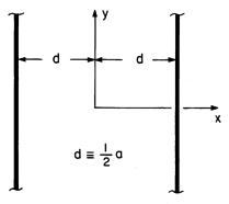 Figure P13.2.2
|
| | TE and TM Standing Waves between Parallel Plates |
|---|
| 13.3.1* | Starting with (13.3.1) (for TM modes) and (13.3.2) (for TE
modes) use steps similar to those illustrated by (5.5.20)-(5.5.26) to
obtain the orthogonality conditions of (13.3.3) and (13.3.4),
respectively.
|
| 13.3.2 | In the system of Example 13.3.1, the wall at y = 0 is replaced by
that shown in Fig. P13.3.2. A strip electrode is embedded in, but
insulated from, the wall at y = 0. The resistance R is low
enough so that E tangential to the boundary at y = 0, even at the
insulating gaps between the strip electrode and the surrounding wall,
is negligible.
| (a) | Determine the output voltage vo in terms of v.
|
| (b) | For b/a = 2, describe the dependence of |vo| on
frequency over the range     a = 0 a = 0 
  5/4, specifying the low-frequency range where the response
has a linear dependence on frequency and the resonance frequencies. 5/4, specifying the low-frequency range where the response
has a linear dependence on frequency and the resonance frequencies.
|
| (c) | What is the distribution of Hz(x, y) at the resonance
frequencies?
|
 Figure P13.3.2
|
| 13.3.3* | In the two-dimensional system of Fig. P13.3.3, each driven
electrode has the same nature as the one in Fig. 13.3.1. The origin
of the y axis has been chosen to be in the plane of symmetry.
| (a) | Use the symmetry to argue that Hz(y = 0) =0.
|
| (b) | Show that in the interior region,

|
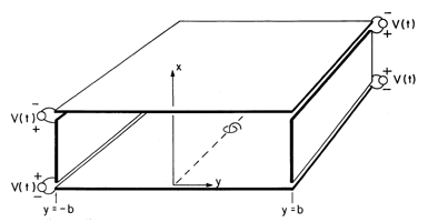 Figure P13.3.3
|
| 13.3.4 | The one-turn loop of Fig. P13.3.4 has dimensions that are small
compared to a, b, or wavelengths of interest and has area A in
the x - y plane.
bottom electrode in Fig. 13.3.1. Assume that the resistance is large
enough so that the current induced in this loop gives rise to a magnetic
field that is negligible compared to that already found. In terms of
Hz, what is vo?
| (a) | It is used to detect the TM H field at the middle of the
|
| (b) | At what locations x = X of the loop is |vo| a
maximum?
|
| (c) | If the same loop were in the plate at y = 0 in the
configuration of Fig. 13.1.3 and used to detect Hz at y = 0 for
the TEM fields of Example 13.1.1, what would be the dependence of
|vo| on the location x = X of the loop?
|
| (d) | If the loop were located in the plate at y = 0 in the
TE configuration of Fig. 13.3.4, how should the loop be oriented to
detect H?
|
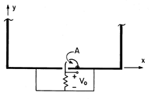 Figure P13.3.4
|
| 13.3.5 | In the system shown in Fig. P13.3.5,   d and the driving
sources v = Re [ d and the driving
sources v = Re [ exp (j exp (j t)] are uniformly
distributed in the z direction so that the fields are
two dimensional. Thus, the driving electrode is like that of Fig.
13.3.1 except that it spans the width d rather than the full width
a. Find H and E in terms of v. t)] are uniformly
distributed in the z direction so that the fields are
two dimensional. Thus, the driving electrode is like that of Fig.
13.3.1 except that it spans the width d rather than the full width
a. Find H and E in terms of v.
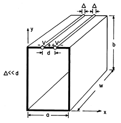 Figure P13.3.5
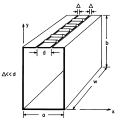 Figure P13.3.6
|
| 13.3.6 | In the system shown in Fig. P13.3.6, the excitation electrode is
like that for Fig. 13.3.4 except that it has a width d rather than
a. Find H and E in terms of  . .
|
| | Rectangular Waveguide Modes |
|---|
| 13.4.1* | Show that an alternative method of exciting and detecting the
TE10 mode in Demonstration 13.4.1 is to introduce one-turn loops as
shown in Fig. P13.4.1. The excitation loop is inserted through a hole
in the conducting wall while the detection loop passes through a slot,
so that it can be moved in the y direction. The loops are each in the
y - z plane. To minimize disturbance of the field, the detection loop
is terminated in a high enough impedance so that the field from the
current in the loop is negligible. Compare the y dependence of the
detected signal to that measured using the electric probe.
 Figure P13.4.1
|
| 13.4.2 | A rectangular waveguide has w/a = 0.75. Presuming that all TE and
TM modes are excited in the guide, in what order do the lowest six
modes begin to propagate in the y direction as the frequency is
raised?
|
| 13.4.3* | The rectangular waveguide shown in Fig. P13.4.3 is terminated in
a perfectly conducting plate at y = 0 that makes contact with the
guide walls. An electrode at y = b has a gap of width   a
and a
and   w around its edges. Distributed around this gap are
sources that constrain the field from the edges of the plate to the
guide walls to v(t)/ w around its edges. Distributed around this gap are
sources that constrain the field from the edges of the plate to the
guide walls to v(t)/ = Re ( = Re ( / / ) exp(j ) exp(j t).
condition at y = 0 to show that t).
condition at y = 0 to show that
 [Hint: If (13.4.9) and (13.4.10) are used, remember that ky = +
 mn for the A+mn mode but ky = - mn for the A+mn mode but ky = - mn for the
A-mn mode. ] mn for the
A-mn mode. ]
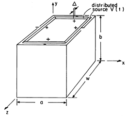 Figure P13.4.3
|
| 13.4.4 | The rectangular waveguide shown in Fig. P13.4.3 is terminated in
a perfectly conducting plate at y = 0 that makes contact with the
guide walls. However, instead of the excitation electrode shown, at
y = b there is the perfectly conducting plate with a square hole
cut in its center, shown in Fig. P13.4.4. In this hole, the pole
faces of a magnetic circuit are flush with the plate and are used to
excite fields within the guide. Approximate the normal fields over
the surface of the pole faces as
 where
where  o is a complex constant. (Note that, if the
magnetic circuit is driven by a one turn coil, the terminal voltage
v = j o is a complex constant. (Note that, if the
magnetic circuit is driven by a one turn coil, the terminal voltage
v = j ( ( 2 /2) 2 /2)  o.) Determine Hy, and hence
E and H, inside the guide. o.) Determine Hy, and hence
E and H, inside the guide.
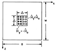 Figure P13.4.4
|
| | Dielectric Waveguides: Optical Fibers |
|---|
| 13.5.1* | For the dielectric slab waveguide of Fig. 13.5.1, consider the
TE modes that have Ez an odd function of z.
ky is again found from (13.5.10), but with (kx d) found by
simultaneously solving (13.5.8) and

| (a) | Show that the dispersion relation between  and and
|
| (b) | Sketch the graphical solution for kx d   m
(m odd) and show that the cutoff frequency is again given by
(13.5.9), but with m odd rather than even. m
(m odd) and show that the cutoff frequency is again given by
(13.5.9), but with m odd rather than even.
|
| (c) | Show that these odd modes also have the asymptote of unity
slope shown in Fig. 13.5.3.
|
| (d) | Sketch the odd mode dispersion relation on that for the
even modes (Fig. 13.5.3).
|
|
| 13.5.2 | For the dielectric slab waveguide shown in Fig. 13.5.1,  i / i / =
2.5, =
2.5,  = =  o, and d = 1 cm. In Hz, what is the
highest frequency that can be used to guide only one TE mode. (Note
the result of Prob. 13.5.1.) o, and d = 1 cm. In Hz, what is the
highest frequency that can be used to guide only one TE mode. (Note
the result of Prob. 13.5.1.)
|
| 13.5.3* | The dielectric slab waveguide of Fig. 13.5.1 is the same as that
considered in this problem except that it now has a permeability
 i that differs from that outside, where it is i that differs from that outside, where it is  .
by .
by


| (a) | Show that (13.5.7) and (13.5.8), respectively, are replaced
|
| (b) | Show that making  i > i >  lowers the cutoff
frequency. lowers the cutoff
frequency.
|
| (c) | For a given frequency, does making  i / i / > 1
increase or decrease the wavelength > 1
increase or decrease the wavelength   2 2 /ky? /ky?
|
|
| 13.5.4 | The dielectric slab of Fig. 13.5.1 has permittivity  i
and permeability i
and permeability  i, while in the surrounding regions these are i, while in the surrounding regions these are
 and and  , respectively. Consider the TM modes.
(13.5.10) that can be used to determine the dispersion relation , respectively. Consider the TM modes.
(13.5.10) that can be used to determine the dispersion relation
 = =  (ky) for modes that have Hz even and odd
functions of x. (ky) for modes that have Hz even and odd
functions of x.
| (a) | Determine expressions analogous to (13.5.7), (13.5.8), and
|
| (b) | What are the cutoff frequencies?
|
| (c) | For  i = i =  and and  i = i =  = 2.5, draw the
dispersion plot for the lowest three modes that is analogous to that
of Fig. 13.5.3. = 2.5, draw the
dispersion plot for the lowest three modes that is analogous to that
of Fig. 13.5.3.
|
|


 y) exp (j
 t).
t).
 o is real and express the standing wave of
(13.1.17) so as to make it evident that it is the sum of
equal-amplitude waves traveling in the
  y directions, each with
a magnitude of phase velocity
  /
/ = c and wavelength
2
 /
/ .
.

 t] at z =
-l.
H.
 t] at x = -l.

 z or
z or  z odd or
even functions of
x. With this in mind, the origin of the coordinate system is moved
so that it is midway between the perfectly conducting plates, as
shown in Fig. P13.2.2.
when the boundary condition is met at x = d
  a/2 for these
functions, it is automatically met at x = -d.


 d and the driving
sources v = Re [
 exp (j
 t)] are uniformly
distributed in the z direction so that the fields are
two dimensional. Thus, the driving electrode is like that of Fig.
13.3.1 except that it spans the width d rather than the full width
a. Find H and E in terms of v.


 .
.


 a
and
a
and 
 w around its edges. Distributed around this gap are
sources that constrain the field from the edges of the plate to the
guide walls to v(t)/
 = Re (
 /
/ ) exp(j
 t).
condition at y = 0 to show that

 mn for the A+mn mode but ky = -
 mn for the
A-mn mode. ]


 o is a complex constant. (Note that, if the
magnetic circuit is driven by a one turn coil, the terminal voltage
v = j
 (
( 2 /2)
2 /2)
 o.) Determine Hy, and hence
E and H, inside the guide.


 i /
i / =
2.5,
  =
=  o, and d = 1 cm. In Hz, what is the
highest frequency that can be used to guide only one TE mode. (Note
the result of Prob. 13.5.1.)
 i that differs from that outside, where it is
  .
by
.
by


 i
and permeability
  i, while in the surrounding regions these are
 and
and  , respectively. Consider the TM modes.
(13.5.10) that can be used to determine the dispersion relation
 =
=  (ky) for modes that have Hz even and odd
functions of x.
 directed and given by I/2


 m
(m odd) and show that the cutoff frequency is again given by
(13.5.9), but with m odd rather than even.
