|
|
|

for 6.111 Introduction to Digital Systems
6.111 home → Labkit home → ChipScope
Debugging with ChipScope
by Daniel Finchelstein and Nathan IckesIntroduction
This document introduces the Xilinx ChipScope Analyzer. ChipScope is a set of tools made by Xilinx that allows you to easily probe the internal signals of your design inside an FPGA, much as you would do with a logic analyzer. For example, while your design is running on the FPGA, you can trigger when certain events take place and view any of your design's internal signals.
Because the ChipScope analyzer logic is implemented in the FPGA, it has some important limitations. The sample memory of the analyzer is limited by the memory resources of the FPGA. In a design that uses much of the FPGA's memory, there may not be much memory left over for the ChipScope cores. Also, ChipScope cannot sample as quickly as an external logic analyzer. Generally, ChipScope sampling rate will be the same as the design's clock frequency. It is therefore not possible to detect glitches with ChipScope.
In order to use the ChipScope internal logic analyzer in an existing design project, you first generate the ChipScope core modules, which perform the trigger and waveform capturing functionality on the FPGA. Afterwards, you instantiate these cores in your Verilog code, and you connect those modules to the signals you want to monitor. The complete design is then recompiled. Instead of loading the resulting .bit file onto the FPGA using iMAPCT, the ChipScope Analyzer application is used to configure the FPGA. ChipScope Analyzer also provides the interface for setting the trigger criteria for the ChipScope cores, and for displaying the waveforms recorded by those cores.
Setting up the Initial Design
This tutorial builds on the simple counter project, described in the Getting Started tutorial. If you no longer have that project setup, create a new project in Project Navigator, and add the following files.
counter.v: thecountermodulelabkit.v: the standard labkit top-level, modified to instantiatecounterlabkit.ucf: the standard labkit constraints file
Synthesize and implement the project now, and try downloading it to the labkit, just to verify that everything is set up properly.
Inserting the ChipScope Cores
Now we will include some ChipScope modules in the counter example in order to allow us to do run-time debugging of the internal signals on the FPGA.
- Launch the ChipScope Core Generator program (Start → Programs → ChipScope Pro 8.2i → ChipScope Pro Core Generator).
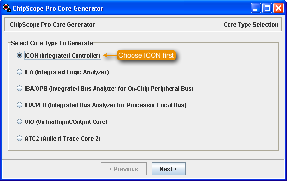
- A dialog box will appear that lets you create the necessary hardware modules for your FPGA. For this tutorial, you will need two different types of modules: ILA and ICON. An ILA is a logic analyzer block which can trigger on internal signals and capture them inside a memory so that they can be viewed through the analyzer GUI. You can have multiple ILA blocks for separate parts of your design. An ICON is a controller module for one or more ILAs. You only need one ICON in your design.
- Select core type to generate: choose ICON, then click "Next".
- Set the output netlist field so that the ICON core is generated in the counter project directory, Make sure the output netlist name ends with
.edn. Make sure Virtex II is selected as the device family. The number of control ports determines how many ILA blocks can be connected to the ICON you are about to generate: choose 1 for this tutorial. Leave the remaining three checkboxes unchecked and click "Next".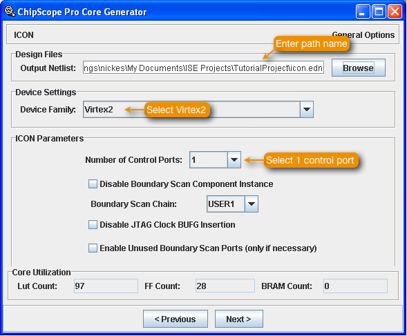
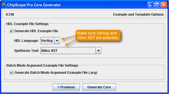
- The next form offers to generate a sample HDL file showing how to instantiate the ICON module. Select Verilog as the HDL language, and make sure Xilinx XST is selected as the synthesis tool. Click "Generate Core" to generate the ICON core files.
- When the ICON core generation is complete, click "Start Over". This time, we will generate an ILA (Integrated Logic Analyzer).
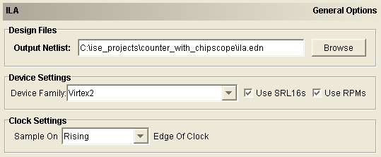
- As with the ICON core, the output netlist should be generated in your project directory, and the device family should be set to Virtex II. Under clock settings, choose to sample on the rising edge of the clock. Click "Next".
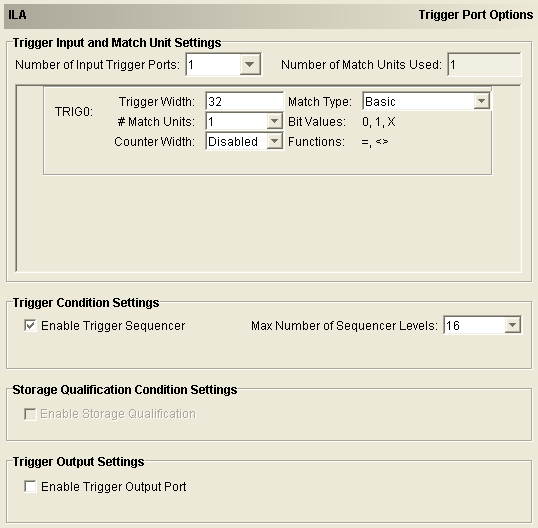
- For Number of trigger ports, choose 1 for now, although for your design you are free to use up to 16. This allows you to have different groups to choose from when you do your triggering at run-time. Under Trig0, choose a trigger width of 32. Match units allow you to create different trigger vectors so that you can trigger on a sequence of different vectors: for example, you might want to trigger only when an address bus changes from 0xAA to 0xBB. For this tutorial, you only need 1 match unit. Leave all other settings at their default values and click "Next".
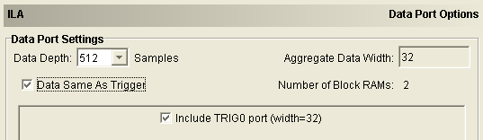
- Choose 512 for data depth. This is the window length for your ILA. The longer it is, the more FPGA memory blocks will be used to implement the ILA core. Select the "Data same as Trigger" box, which allows you to view all the signals of interest, as well as to potentially trigger on all of them. Click "Next".
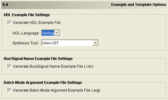
- Make sure the language for the generated example HDL file is set to Verilog, and Xilinx XST is selected as the synthesis tool. Click "Generate Core".
- In your project directory, you should now have a number of new files
icon.edn: The pre-synthesized EDIF netlist for the ICON core.icon.ncf: Synthesis constraints for the ICON coreicon_xst_eaxmple.v:: Example Verilog code showing how to instantiate the ICON core. This file also provides a dummy "black-box" definition of the core.ila.edn: The pre-synthesized EDIF netlist for the ILA core.ila.ncf: Synthesis contraints for the ILA coreila_xst_example.v: Example Verilog code showing how to instantiate the ILA core, and a dummy "black-box" definition of the core.
- You have now generated all the necessary ChipScope hardware blocks, and are ready to include them in the existing counter design. Start Project Navigator, and open the counter project. Open the
labkit.vfile within Project Navigator. - Just before the end of the
labkitmodule, add the following lines of Verilog code to instantiate the ICON and ILA coreswire [35:0] control0; icon icon1 (.control0(control0)); ila ila1 (.control(control0), .clk(clock_27mhz), .trig0(count));
The ILA and ICON modules are connected by a 36-bit bus (control0). If your design had multiple (up to 15) ILA modules, each would be connected to a different control port on the ICON, using a unique 36-bit control bus. Thetrig0port on the ILA should be connected to the signals that you wish to probe with the ChipScope analyzer. - At the end of the
labkit.vfile (after theendmodule), copy the black-box definitions of the ICON and ILA cores, from the*_xst_example.vfiles. The black-box definitions will look like thismodule icon ( control0 ); output [35:0] control0; endmodule module ila ( control, clk, trig0 ); input [35:0] control; input clk; input [31:0] trig0; endmoduleThe ICON and ILA cores have already been synthesized. During the "Translate" portion of the design compilation process, the.ednfiles for the ICON and ILA cores will be read in and combined with the remainder of the counter project. The black-box definitions above are necessary to tell the synthesis tool (XST) what the ports of the ICON and ILA modules are. The functionality of these modules will be filled in when the.ednfiles are read. - Make sure the top-level module
labkitis selected in the source tree, and double-click on "Generate Programming File in the processes window, to compile the design. - Connect the programming cable to the JTAG port on the labkit, and power on the labkit. Instead of using iMPACT to download the
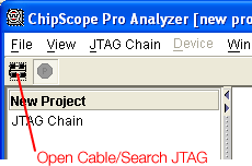
.bitfile to the labkit, launch the ChipScope Pro Analyzer application (Start → Programs → ChipScope Pro 6.1i → ChipScope Pro Core Analyzer). - Inside ChipScope Analyzer, click on the left-most toolbar button ("Open cable/Search JTAG")
- ChipScope should detect three devices on the JTAG chain. Click "OK".
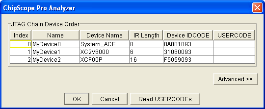
- In main ChipScope window, right-click on "DEV:1 MyDevice1 (XC2V6000)" and choose "Configure...". Click "Select New File" in the dialog that appears, and then select the
labkit.bitfile in the counter project directory. - Click "OK" to dismiss the "Configur..." dialog. ChipScope will begin downloading the
.bitfile to the labkit. (Watch the progress indicator in the lower-right corner of the ChipScope window.) When the download completes, the LEDs on the labkit should start counting. - Click on the "T!" button in the ChipScope toolbar to force the analyzer to trigger immediately. The waveform window will display the captured waveforms.
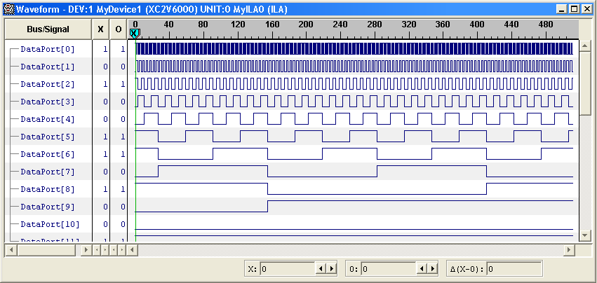
- To group analyzer channels into a bus, expand the "Data Port" item in the window pane labeled "Signals: DEV: 1 UNIT: 0"
Select all 32 signals, then right-click and select "Add to Bus" → "New Bus". Name the new bus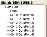
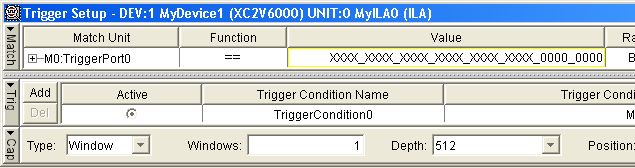
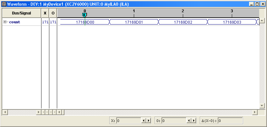
count. Right-click and select "Clear All" → "Waveform". Then right-click on the name of the new bus and select "Add to View" → "Waveform". The waveform window should now only contain the 32-bit buscount. - Now, let's change the trigger setup to trigger when the lower eight bits of the count bus are all zero. In the Trigger Setup window, highlight the last eight "X"s of the value field. Type eight zeros, and then return.
- Click the play button in the ChipScope toolbar to arm the analyzer, and wait for a trigger event. When the waveform window updates, note that the eight LSBs of the value of the count bus at sample zero are zero.
Solutions to Common Problems
- Adding ChipScope cores to a design causes place-and-route errors such as "
ERROR:DesignRules:10 - Netcheck: The signal "U_ila_pro_/i_no_d/u_ila/u_trig/u_tm/g_nmu/0/u_m/u_mu/i_mut_gand/u_match/cfg _data_63" is completely unrouted."This is a known bug in ChipScope 6.3i. See Xilinx Answer Record 20435, which recommends the following workarounds:
- Regenerate the ChipScope cores with the RPM option disabled.
- Change the match type from "Basic" to "Basic w/edges".
- Change the trigger width to a number that, when divided by eight, does not leave a remainder of 1, 2, 3, or 4. For example if your Trigger Width is 20, change it to 21.
MIT 6.111 Introduction to Digital Systems, Updated February 05, 2007