|
|
|

for 6.111 Introduction to Digital Systems
6.111 home → Labkit home → ZBT SRAM Interface
ZBT SRAM Interface
The easiest way to implement memory on the labkit, is to use the FPGA's built-in SRAM blocks. However, some designs may require more memory than is available inside the FPGA.
The labkit contains two synchronous, 512k x 36 ZBT SRAM chips (on the back side of the PCB). These are relatively high-speed devices (up to 167MHz), but they can be somewhat tricky to interface to.
ZBT Interface Protocol
The ZBT memories are synchronous: they require a clock input, and their inputs are only sampled on the rising edges of that clock. They are also pipelined, with the data bus being delayed by two cycles after the address and control signals. In other words, if a read cycle is initiated (~CE and ~OE are low, ~WE is high, and the address is valid) on clock cycle n, then the data read from that address will be available on cycle n+2. Similarly, for a write cycle, the data to be written is supplied on cycle n+2.
The ZBT memories have the following control signals:
- Clock input (CLK): All memory interface signals except output enable (~OE) are synchronous to the rising edge of this clock.
- Clock enable (~CEN): When high, transitions on the CLK are ignored. Most designs will hold ~CEN low all the time.
- Chip enables (~CE1, CE2, ~CE3): These signals must all be in their active states in order to enable a memory access. The CE2 and ~CE3 inputs are hard wired on the PCB, so only ~CE1 can be controlled by the FPGA.
- Output enable (~OE): When high, the databus is tristated. During a write, the databus is automatically tristated during the cycle when the data is to be supplied, so it is safe to keep ~OE low all the time. ~OE is an asynchronous input: it affects the data bus immediately. (It's not pipelined.)
- Write enable (~WE): When low, selects a write cycle; when high, selects a read cycle.
- Byte write enables (~WEA, ~WEB, ~WEC, ~WED): Each of these enable signals controls nine bits of the databus, allowing partial word writes.
- Advance/load (ADV/~LD): This signal controls the internal "burst mode" address counter. When ADV/~LD is low, the address used for a memory cycle comes from the address input pins. When ADV/~LD is high, the address from the previous cycle is incremented and used as the address for the current cycle. Note that the counter is only two bits wide, so burst accesses are limited to four cycles. For most applications, it is easiest to avoid burst mode entirely.
The figure below illustrates normal read and write transactions (e.g., not using burst mode) for the ZBT memories. The same clock is used by both the FPGA logic and the RAMs. (More about that in the next section.)
ZBT memory access protocol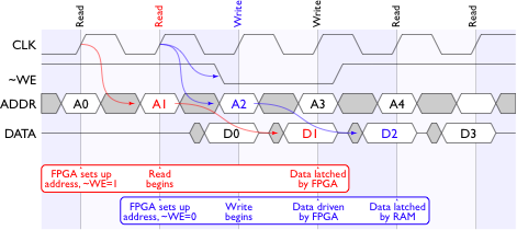
Clock, chip, output, and byte-write enable signals are all held low (active) throughtout the above transactions.
Memory Clock Generation
Inside the FPGA, clocks are distributed using dedicated clock trees, which ensure that the clock signals reach every flip-flop relatively simulataneously. If the clock inputs of the ZBT memories are driven by outputs of the FPGA, then the clock signal at the memories will be delayed by the sum of the propagation delay through the FPGA output pins and the propagation delay of the PCB trace.
To correct this skew at the memory devices, we need to drive the ZBT clock inputs with a phase-shifted version of the clock, so that the rising clock edge reaches the memory devices at the same time that it reaches all the registers in the FPGA. To generate this phase-shifted clock, a delay-locked loop (DLL) is used. DLLs are fundamentally analog components. There is no way to infer a DLL using Verilog code, so they must be instantiated. The Xilinx libarary component containing a DLL is the digital clock manager, or DCM.
The following is a high-level and incomplete description of the operation of DCMs. For more information, see the Libraries Guide volume of the Xilinx documentation. Essentially, a DCM takes a reference clock input signal on its CLKIN port, and outputs a delayed copy of that clock on its CLK0 output port. The CLK0 output is generally used to drive a clock distribution tree (a BUFG primitive in the Xilinx library). One output of the clock distribution tree should be used to drive the feedback input (CLKFPB) of the DCM. The delay between the CLKIN and CLK0 ports on the DCM is automatically adjusted by a feedback loop until the CLKIN and CLKFB inputs are in phase. Once the phase difference between CLKIN and CLKFB has been minimized, the DCM is said to be "locked", and outputs of the clock distribution tree should be exactly in phase with the input clock signal. Effectively, the propagation delay through the clock distribution tree has been canceled, because the total propagation delay from the CLKIN pin of the DCM to the output of the clock distribution tree is exactly one clock period.
The schematic below shows how two DCMs can be used to ensure that the ZBT memories are clocked at exactly the same time as the FPGA flip-flops.
ZBT memory clock de-skew circuitry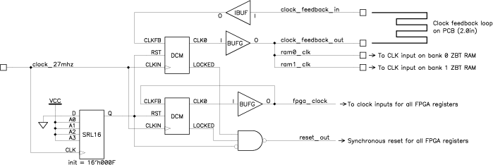
In the circuitry above, the lower DCM is used to ensure that the fpga_clock signal, which clocks all of the FPGA flip-flops, is in phase with the refence clock (clock_27mhz, in this example). The upper DCM is used to generate the de-skewed clock for the external ZBT memories. The feedback loop for this DCM includes a 2.0 inch long trace on the labkit PCB. Since all of the PCB traces from the FPGA to the ZBT memories are also 2.0 inches long, the propagation delay from the output of the upper DCM back to its CLKFB input should be almost exactly the same as the propagation delay from the DCM output to the ZBT memories.
The 16-bit shift register (SRL16) is used to ensure the DCMs lock properly when the FPGA finishes its configuration process. During configuration, the FPGA's I/O pins are all held in tristate. The DCMs are released from reset a few clock cycles before the global tristate signal is released. The upper DCM therefore attempts to lock without a feedback input. It is possible for the DCM to get stuck in a funny state, and never properly lock. To prevent this, a shift register is used to trigger a reset of both DCMs shortly after the entire FPGA configuration proccess is complete and the I/O pins have been enabled.
The LOCKED output of a DCM signals that the feedback loop on the DCM's internal DLL has stabilized. The reset_out signal in the circuit above should be used as an active-high reset signal for any logic driven by fpga_clock.
Verilog code implementing this circuitry is available here. Note that, in order to minimize routing delay on the clock signals, this code utilizes input clock buffers (IBUFG) for both the reference clock and feedback inputs. It also utilizes I/O flip-flops (OFDDRRSE) for the RAM and feedback clock outputs. These special primitives are actually part of the I/O driver circuitry on the FPGA. This means that you will not be able to use these inputs or outputs anywhere else in your code, because the IBUFG and OFDDRRSE gates place these signals outside of the range of the general routing mesh.
More Information
- Xilinx application note XAPP136: Synthesizable 200MHz ZBT SRAM Interface
- Datasheet for the Cypress CY7C1370C 512Kx36 pipelined ZBT SRAM
MIT 6.111 Introduction to Digital Systems, Updated April 26, 2007