Sensing Circuit
By Tiankai Chen
The crux of the game is to be able to sense which state or position each jar is in. For the concept refinement, I explored three different design iterations.
The first design is a naive circuit that is a hassle to wire and create. The second design is based off the keyboard matrix and is an elegant solution that greatly reduces the amount of circuitry required. The third design improves on the second design with a voltage divider circuit, reducing the circuitry required.
For this assignment, I also wrote the Gameplay for the team.
Introduction to Jar Circuit

The circuitry in the jar can be explained by a single pole and 4 throw switch. As each jar has 4 different faces, it has 4 possible states. At any one time, the jar would be in one of the 4 states. More information on the mechanical and electrical workings of the jars can be found here.
Design 1: Naive Circuit

The basics behind sensing the state of one switch is shown in the figure on the left. A represents the voltage input while B represents a standard IO pin on a microcontroller that is able to read a "high" or "low" state.
When the switch is open, B would register a "low" state as it would have the same voltage as the ground. When the switch is closed, the current flows from A to the ground and B would register a "high" state as it would have the same voltage as the input voltage.
As a single jar has 4 throws, a single jar would have 5 wires leading into it. We can imagine that with a total of 40 jars on one wall, we would need a total of 200 wires to connect the switches to a microcontroller. You would also require 200 IO pins.
Even if we were to decentralize each jar's circuit to have a microcontroller for each jar, it would still involve a lot of wiring and circuit boards. This concept is illustrated in the figure below. More details on how the jars are arranged on the wall can be found here.
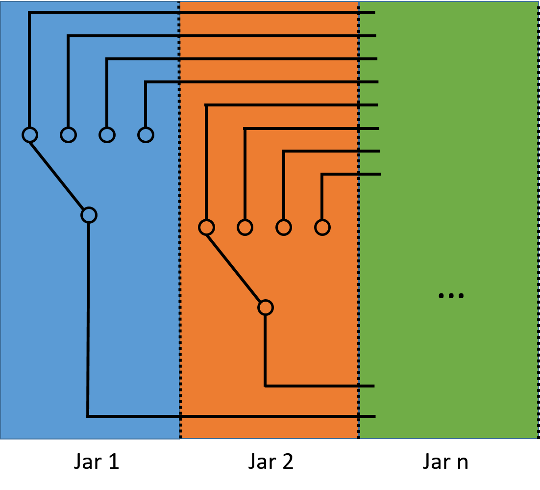
Design 2: Matrix Circuit

This matrix circuit design is based off the circuit used in keyboards. A keyboard is basically a matrix of many switches and it was imperative to simplify the circuitry back then. It achieves this by using a matrix circuit. The basic circuit diagram largely remains the same with the addition of a diode to ensure that current only flows in a single direction. The rationale behind the diode is explained later on.
The matrix circuit can be observed in the circuit diagram below. A1, A2, ... represents the rows while B1, B2, ... represents the columns. A single row represents each shelf while the columns represents all the switches on each shelf.

The matrix circuit works be sequentially scanning each switch at the (A,B) coordinates. For example, to check the state of switch(A1,B2), A1 is thrown to "high" while B2 attempts to read the voltage. Due to the open switch at position (A1,B2), B2 would read a "low" state. This repeats for each column followed by each row.
Although it is not represented in the figure above, one jar involves 4 of the switches in 1 row. Hence, there are 5 rows and 8*4 columns. This would require 37 main wires and IO pins, greatly simplifying the circuitry. Furthermore with a 16MHz microcontroller, we can easily scan the whole matrix thousands of times per second, ensuring that there are no lag in the responses.
Ghosting

Without any diodes in the circuit, a phenomenon called ghosting occurs when multiple keys in the same row and column are pressed. As shown in the figure, when the switch at position (A1,B1) is being checked, the current is able to pass through the 3 closed switches giving a false positive to B1.
This may not be as big of an issue with keyboards as one key is usually pressed at a time. However, this would be a huge problem in our game as many switches would be closed at any point in time. However, with a diode behind each switch, we would prevent this phenomenon from occuring.
Design 3: Matrix VD Circuit

The previous two circuit design only allows a binary check at B. It is either "high" or "low". However, with the addition of a voltage divider circuit, the voltage reading at B can be can be used to identify 4 different states. For example, a reading of 2*V/4 will indicate switch A2 is closed while a reading of V will indicate switch A4 is closed (V is the voltage input across A1 to A4). The resistor values (R,R1,R2,R3,R4) can be easily chosen to provide a good ratio.
The updated circuit diagram is shown below. A1, A2, ... represents the rows while B1, B2, ... represents the columns. A single row represents each shelf while each column represents a column of jars.

As mentioned before, it scans each location sequentially. For example, A1 is thrown to "high" while B2 attempts to read the voltage. Due to the closed switch with a resistance of R1, B2 would read a corresponding ratio of the voltage input, indicating 1 of the 4 states. This repeats for each column followed by each row.
This voltage divider circuit reduces the number of circuitry required with the addition of very simple electrical components. Now, only 13 main wires and IO pins are required.
Conclusion
In conclusion, the 3 design iterations have explored different ways of approaching this problem. The final design only requires 13 main wires and IO pins for a single wall of jars. The actual wiring into a microcontroller is pretty simple, involving only the IO pins. However, for the third design, Analog pins are required to measure the voltage relative to the voltage input.
However, there are some concerns regarding the third design. As it relies heavily on the ratio of resistances to separate the different states, there are chances in which it would give errors.
In reality, the electrical surface contacts for the jar would have its own contact resistance which may change over time. For example, repeated turning of the jars may cause the total resistance at a throw to change. This may cause false positives that would spoil the experience for the players. The best foolproof method would be design 2 that has already improved greatly since design 3.