Porsche Anti-Theft System
A recent MIT grad just completed a very successful IPO of her Cambridge startup and celebrated by purchasing a new Porsche. Though the car has a built in anti-theft system, she is concerned since this is a standard factory unit and many people know how to disable it. So she's looking for someone to design and build a system with some hidden security features only you two will know about! Your job is to create a working prototype.
In this lab you will implement an anti-theft system that uses several interacting FSMs to process sensor inputs and generate the appropriate actuator control signals. This lab provides you with a design methodology that will be useful in future labs and your final project.
Procedure
- Read through the lab to understand the desired functionality, determine your approach and complete a design. Although not required, you may find it helpful to schedule a conference with a member of the course staff to review your design. This will help catch any major mistakes early in the process.
- Prototype your design using the labkit. After you verify the anti-theft system's functionality get a member of the course staff to check you off. Be ready to demonstrate the functionality of your implementation and to answer the questions proposed in the Checkoff List section above.
Description of Anti-Theft System
Since your client is completely focused on her start-up, she wants an anti-theft system that's highly automated. The system is armed automatically after she turns off the ignition, exits the car (i.e., the driver's door has opened and closed) and T_ARM_DELAY has passed. If there is a passenger and both the driver's door and passenger's doors are open, the system arms itself after all the doors have been closed and T_ARM_DELAY has passed; that delay is restarted if a door is opened and reclosed before the alarm has been armed.
Once the system has been armed, opening the driver's door the system begins a countdown. If the ignition is not turned on within the countdown interval (T_DRIVER_DELAY), the siren sounds. The siren remains on as long as the door is open and for some additional interval (T_ALARM_ON) after the door closes, at which time the system resets to the armed but silent state. If the ignition is turned on within the countdown interval, the system is disarmed.
Always a paragon of politeness, your client opens the passenger door first if she's transporting a guest. When the passenger door is opened first, a separate, presumably longer, delay (T_PASSENGER_DELAY) is used for the countdown interval, giving her extra time to walk around to the driver's door and insert the key in the ignition to disarm the system.
There is a status indicator LED on the dash. It blinks with a two-second period when the system is armed. It is constantly illuminated either the system is in the countdown waiting for the ignition to turn on or if the siren is on. The LED is off is the system is disarmed.
So far this all is ordinary alarm functionality. But you're worried that a knowledgable thief might disable the siren and then just drive off with the car. So you've added an additional secret deterrent -- control of power to the fuel pump. When the ignition is off power to fuel pump is cut off. Power is only restored when first the ignition is turned on and then the driver presses both a hidden switch and the brake pedal simultaneously. Power is then latched on until the ignition is again turned off.
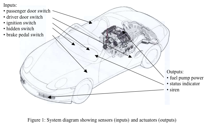
The diagram below lists all the sensors (inputs) and actuators (outputs) connected to the system.
The system timings are based on four parameters (in seconds): the delay between exiting the car and the arming of the alarm (T_ARM_DELAY), the length of the countdown before the alarm sounds after opening the driver's door (T_DRIVER_DELAY) or passenger door (T_PASSENGER_DELAY), and the length of time the siren sounds (T_ALARM_ON). The default value for each parameter is listed in the table below, but each may be set to other values using the Time_Parameter_Selector, Time_Value, and Reprogram signals. Time_Parameter_Selector switches specify the parameter number of the parameter to be changed. Time_Value switches are a 4-bit value representing the value to be programmed -- a value in seconds between 0 and 15. Pushing the Reprogram button tells the system to set the currently selected parameter to Time_Value. Note that your system should behave correctly even if one or more of the parameters is set to 0.
| Interval Name | Symbol | Parameter Number | Default Time (sec) | Time Value |
|---|---|---|---|---|
| Arming delay | T_ARM_DELAY | 00 | 6 | 0110 |
| Countdown, driver's door | T_DRIVER_DELAY | 01 | 8 | 1000 |
| Countdown, passenger door | T_PASSENGER_DELAY | 10 | 15 | 1111 |
| Siren ON time | T_ALARM_ON | 11 | 10 | 1010 |
Block Descriptions/Implementation
The following diagram illustrates a possible organization of your design into modules.

You should implement this lab by programming each module individually and then instantiating and connecting the modules together in the toplevel labkit.v module. Then compile your implementation using the Xilinx tools, download it to your kit's FPGA, and demonstrate its operation. Please use the following labkit devices for the various sensors and actuators:
| Sensor/Actuator | Labkit device |
|---|---|
| Hidden switch | button0 |
| Brake depressed switch | button1 |
| Driver door switch | button2 |
| Passenger door switch | button3 |
| Ignition switch | switch[7] |
| Time_parameter_selector | switch[5:4] |
| Time_value | switch[3:0] |
| Reprogram | button_enter |
| Status light | led[0] |
| Fuel pump power | led[1] |
| Siren output | user1[0] |
| System reset | button_down |
Here's a more detailed description of each module:
- Debouncer
-
Your clocked state machine is controlled by several asynchronous
inputs that might be changed by the user at any time, potentially
creating a problem with metastability in the state registers if one of
the inputs changes too near a rising clock edge. In general
asynchronous inputs need to be synchronized to the internal clock
before they can be used by the internal logic. synchronize.v
(available on the Handouts page of the course website) is a Verilog
implementation of a pulse synchronizer that can convert an
asynchronous signal to a synchronous one with acceptably low
probability of metastability in the synchronous signal.
A second problem arises from the mechanical "bounce" inherent in switches: as a metal contact opens and closes it may bounce a couple of times, creating a sequence of on/off transitions in rapid succession. So you need to use debouncing circuitry to filter out these unwanted transitions. debounce.v (available on the Handouts page of the course website) is a Verilog implementation of a digital retriggerable one-shot that requires that an input transition be stable for 0.01sec before reporting a transition on its output. This module happens to produce a synchronous output, so a separate synchronizer is not required. You should use an instance of the debounce module to debounce any switch inputs you use in your design.
- Time Parameters
-
The time parameters module stores the four different time parameter
values. The module acts like a 4-location memory that's initialized
with default values at power on, but may be reprogrammed by the user
at any time. Using the 2-bit Interval signal, the Anti-theft FSM
selects one of the four parameters to be used by the Timer module.
On power on, the parameters should be set to the default values specified above. However the user may modify any of the values by manipulating Time_Parameter_Selector (2 bits), Time_Value (4 bits), and Reprogram. Whenever a parameter is reprogrammed, the FSM should be reset to its ARMED state (after which it may transition immediately to another state depending on the sensor inputs).
- Divider
- The divider converts the 27MHz master clock into an one_hz_enable signal that's asserted for just 1 cycle out of every 27,000,000 cycles (i.e., once per second). The one_hz_enable is used by the Timer module and for making the LED blink with a two-second period. The divider needs to reset when Start_Timer is asserted (see Timer module below) so that the first one_hz_enable after the timer starts to count comes a full second after the timer has been started.
- Timer
- The timer counts down the number of seconds specified by the Time Parameter module. It initializes its internal counter to the specified Value when Start_Timer is asserted and decrements the counter when one_hz_enable is asserted. When the internal counter reaches zero, the Expired signal is asserted and the countdown halts until Start_Timer is once again asserted.
- Anti-theft FSM
-
This finite state machine controls the sequencing for the system. The
system has four major modes of operation:
- Armed. The status indicator should be blinking with a two-second period; the siren is off. If the ingition switch is turned on go to Disarmed mode, otherwise when a door opens start the appropriate countdown and go to Triggered mode. This is the state the FSM should have when the system is powered on.
- Triggered. The status indicator light should be constantly on; the siren is off. If the ignition switch is turned on, go to Disarmed mode. If the countdown expires before the ignition is turned on, go to Sound Alarm Mode.
- Sound Alarm. The status indicator light and siren should be constantly on. The alarm should continue to sound until either T_ALARM_ON seconds after all the doors have closed (at which point go to Armed mode) or the ignition switch is turned on (at which point go to Disarmed mode).
- Disarmed. The status indicator light and siren should be off. Wait until the ignition switch is turned off, followed by the driver's door opening and closing, then after T_ARM_DELAY seconds go to Armed mode.
Note that more than one FSM state may be needed to implement the required functionality of each mode, i.e, your state transition diagram will have many more than 4 states.
- Fuel Pump Logic
- This simple FSM controls the power to the fuel pump. Power is disabled when the ignition switch is turned off and only reenabled when the appropriate sequence of sensor values is received (see description above).
- Siren Generator
- This module generates an audio-frequency square wave (i.e., a
sequence of alternating 0's and 1's) that can be used to drive an
external speaker. At a minimum your generator should alternate
at couple of second intervals between a 400Hz tone and a 700Hz tone.
But fancier effects are possible -- see below.
Connect the output of the siren generator to the user1[0] output of the FPGA, which appears on a connector at the top of the labkit board. Use a wire to connect that signal to the breadboard and use a couple of resistors as shown in the block diagram above to create a circuit on the protoboard where you can connect up the auxillary input of the external Radio Shack speaker box (there should be 12 speaker boxeskicking around the lab -- check over by the TA table). Note that the speakers have their own power supply module which must be plugged in order for the speakers to work.
You're anxious to make a good impression on your client in the hopes of getting the design commisions. So once you've implemented the basic functionality described above, create a different sound effect with your Siren Generator. Some ideas:
- sweep the frequency of the audio tone from 400Hz to 700Hz (or vice versa) and then repeat. Produces a repeating rising/falling tone instead just alternating between the two frequencies.
- produce a warbling tone (rapidly switch between a couple of frequencies).
- Alternate between a tone and silence.
- Sequence through different effects.
Labkit.v
The labkit.v template top-level file can be downloaded by right-clicking on the link and choosing "Save As". Labkit.v allows a user to utilize all of the labkit features including buttons, switches, leds, logic analyzer pins, user input/output pins, audio video capabilities, etc.
You will need to instantiate all submodules in this top level file as well as create wires to connect the submodules. For example, to connect and instantiate your divider and timer blocks you could add something like the following lines in the labkit.v file:
//declare wires as shown in Figure 2 to connect the submodules:
wire reset_sync;
wire one_hz_enable;
wire [3:0] value;
wire expired, start_timer;

//instantiate the submodules and wire their inputs and outputs
//(use the labkit's clock_27mhz as the clock to all blocks)
divider divider1 (.clock_27mhz(clock_27mhz), .reset_sync(reset_sync),
     .one_hz_enable(one_hz_enable));
timer timer1(.clock_27mhz(clock_27mhz), .reset_sync(reset_sync), .value(value),
     .expired(expired), .start_timer(start_timer));
In addition, you will need to connect the input buttons and switches that you use to the appropriate submodules. There are verilog statements in labkit.v that set default values for all outputs, e.g., the leds and user1[0]. You'll need to replace those statements with your own logic that generates the appropriate driving values.
Debugging
Inevitably your design won't be 100% correct the first time. Debugging by just observing the outputs talked about above may not work -- you'll need more info to figure out what's happening. Start by building a test-jig for each module of your design and then the overall test-jig to verify the expected behavior of the system on several sequences of inputs that you expect to test on a real labkit. Once the system passes these tests you can proceed to the implementation on the labkit.
For debug on the labkit you have several options. Use the display_16hex.v module (available on the Handouts webpage) to show 16 hex digits of info (64 bits) on the labkit's 16-character flourescent display. You will need the display to show that your timer is working correctly. Use one digit to show the current state of the FSM, another digit to indicate currently selected time parameter, yet another digit to show the current value of the timer's module internal counter, etc. You'll want to use this handy module for displaying debugging info for all your designs!
Another useful tool for capture sequences of debugging data is the logic analyzer. There are adapter cards that hook the analyzer data pods directly to the FPGA signals analyzer1_data[15:0] (pods A0 and A1) and analyzer3_data[15:0] (pods A2 and A3). The FPGA signal analyzer1_clk is hooked to CK1 of the logic analyzer and analyzer3_clk is hooked to CK0. See analyzer_mapping.pdf for a diagram of the connections.