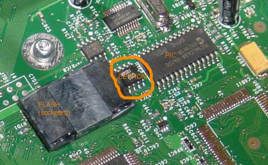
Socket for your TSOP FLASH (29F080A-70) in the Xbox)
I figure there are a lot of great software hackers out there going at the xbox to put linux on it (okay so this is written within a week after its intro, so give me a break if this is out of date). I'm more of a hardware-type, so here's my tiny contribution to the effort.
An interesting anecdote, btw, is that when Microsoft came by MIT to give the X-BOX/recruiting presentation to the students here, we asked the guy (I forget his name, but he was important--I do recall he claimed to help define the DHCP spec :-P) if they had any plans on making it tough to hack the boxes and run linux. They dude looked honestly surprised and it hadn't even crossed his mind. This was about six months or so before the X-BOX launch. There's some commentary at the bottom of this page on the legal aspects of reverse engineering.
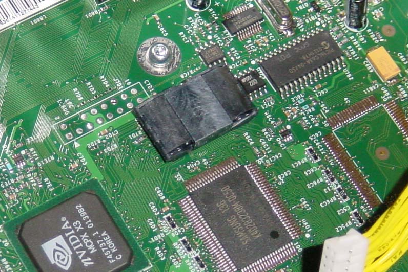
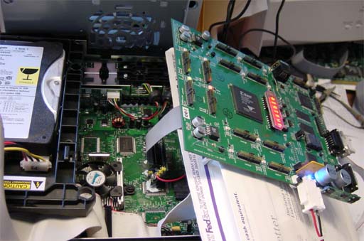
Anyways, something useful during the reverse engineering phase is always having the ability to pull out the BIOS ROM and stick your own in. Except on the X-BOX it ain't socketed. My recommendation is to install an Emulation Technologies S-TS-SM-040-A (if they don't have those in stock, the bigger sockets work too--I put a 48 pin socket on my board 'coz that's what I had on hand tonight). It's a pretty economical device, $12 or so and it goes right in the original footprint on the board.
This is what the socket looks like when in the "open" position: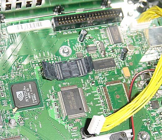
When it's closed, it looks like this:
You need the following to do this: tongs-style soldering iron (to remove the existing flash device), a fine-tipped soldering iron, a microscope, flux, and some solder paste is always nice, but you can use just plain old fine solder too. If you don't have tongs-style soldering iron, you can just cut the device off the board if you have extras laying around (presumably you also have a ROM burner--I use the Needham's Electronics EMP series) or you can build your own (I built an improved version but I haven't got the docs on the web yet...)
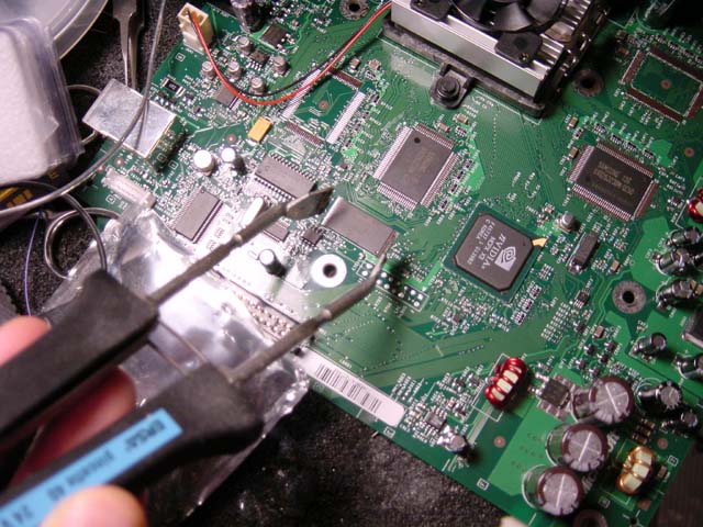
Be sure to clean and recondition the board after removing the ROM before attaching the socket. Be careful about bridging on the socket pins, too, while soldering. If you have a bridge, some flux and chem-wik will usually take care of it. You also have to recondition the ROM before using it in the ROM burner (this is probably the hardest part). Use a fine-tipped soldering iron to remelt the solder on every pin, and clean the device off with some defluxing agent.
For those of you looking to get the ROM contents of the Nintendo gamecube, it's not as easy as the Xbox. Their motherboard has no generic FLASH or recognizeable ROM part on it; my current suspicion is that it's part of a multi-chip package (or maybe even integrated into the same die--that's unlikely, though, due to the volatility of ROM code as the console matures). I'm guessing the "ARAM" chip contains the ROM (probably a synchronous interface ROM so it can share a common bus easily with an SDRAM) and the "slow" SDRAM in a combo package...maybe I'll sacrifice a GameCube for the sake of curiosity and dissolve the package with hot sulfuric or better yet try and shave the package down so I can extract the pinout through visual inspection. I also noticed that the same pins that go to the "high-speed expansion port" appear to go straight from the ARAM chip to a connector, so perhaps an o-scope plus a peripheral that plugs into the port will lend clues...if anyone has any info, I'd be curious to hear it.
Tidbits
I'm just your basic yokel poking at a console...so...caveat hacker... use all the following knowledge at your own risk! Sorry about the formatting. It's pretty much an as-it happens running account of my experiences with the console. More recent stuff is near the bottom.
A tip for those who are trying to extract the ROM images--there are in fact four identical 256k copies of the ROM image in the 1 MB flash ROM. It threw me off at first, I thought perhaps my top two address pins were stuck, but I re-burned the image I obtained into the ROM (same ROM, no copies were made, ftr ;-) and the Xbox boots just fine. A friend (whose identity I'll keep anonymous) insightfully points out that this is quite a reasonable thing to do for adding robustness to the process of FLASH upgrades in the field, and for keeping multiple versions of the BIOS around in case different games rely on features or even bugs found in previous BIOS versions.
Another tidbit on the BIOS image is that with winzip compression, the BIOS image (originally 1024k) compresses down to 1004k. This indicates that a large part (but not necessarily all) of the data in the BIOS is either compressed and/or encrypted (executeable binaries usually compress pretty well). It is also my opinion upon cursory inspection of the ROM images that no address/data pins were swapped or scrambled on the ROM.
A fellow at U Texas (identity kept anonymous) points out to me that MS gave a talk at their university, and the speaker said that they did implement some security measures to foil hackers that try to run a different OS on the Xbox. The speaker mentioned something about desoldering three chips. One is most likely the FLASH. My guess is if this information is true, there is a PIC 16LC63A microcontroller right next door to the FLASH...I wouldn't be surprised if the PIC microcontroller monitors the FLASH to make sure the right sequence of operations happens, and halts the processor if something is amiss. The third chip...well, no guesses on that one yet. Hopefully it's not the nVIDIA MCPX. :-) The speaker at this talk also indicated that the kernel on the Xbox is a much-stripped-down Win2k derivative (from 12 MB to around 23kB). note: it is now known that the PIC does not monitor the FLASH during boot and does little more than coordinate system management activities.
Early BIOS extraction and disassembly
There's an issue with the BIOS decryption that we've encountered-- data in the BIOS does not decrypt by just running the code on a conventional machine using the straight Xbox binaries.
Thanks to Roastbeef for theory (1) and for providing help with disassembly and interpretation of the code.
The two current theories in progress are:
1) byte accesses have their data bits scrambled (while DWORD accesses (cache-line fills
for code, etc) do not)
2) some mid-range address bits are scrambled and/or inverted and/or an offset has been applied
I've gone through the decryption routine of the BIOS
finally, and it is a derivative of RC-4. It sets up
an S-box similar to RC-4:
caveat hacker: this code may or may not be correct (but let me know if you do find a bug :-)
THIS CODE IS KNOWN TO BE BOGUS, AS THE BOOT SECTOR IN THE FLASH ROM IS BOGUS AND GETS OVERRIDEN BY A BLOCK IN THE MCPX
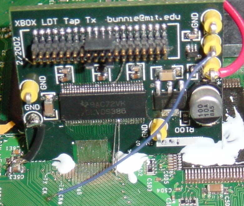
One can tap the LDT bus to find the "proper" code.
  unsigned char K[256]; // 0xFFFFC80 in flash
  unsigned char S[256]; // 0x10000 in SDRAM

  // initialize keys similar to RC-4
  for( i = 0; i < 256; i++ ) {
    S[i] = i;
  }

  j = 0;
  for( i = 0; i < 256; i++ ) {
    j = (j + K[i] + S[j]) % 256;  // RC-4 would do j = (j + K[i] + S[i]) % 256

    // swap S[i], S[j]
    temp = S[i];
    S[i] = S[j];
    S[j] = temp;
  }
The S-box is a permutation of the numbers 0-255; the
key is used to scramble up the order of the numbers. You
can check if you did the S-box generation correctly by
verifying that every number is in there exactly once.
Now, RC-4 would then use this S-box to generate random numbers in a manner that evolves with the encryption stream, but is independant of the ciphertext. The x-box version of this evolves the S-box with feedback from the ciphertext:
  unsigned char cipherText[16384]; // 0xFFFFA000 in FLASH
  unsigned char plainText[16384];  // 0x400000   in SDRAM

  for( index = 0x4000, i = 0, k = 0; index > 0; index-- ) {
    // xbox version
    t = (S[i] ^ cipherText[k]) % 256;
    plainText[k] = t;

    // swap( S[i], S[t] );
    temp = S[i];
    S[i] = S[t];
    S[t] = temp;

    i = (i + 1) % 256;
    k++;
  }
how is this significant? well,
1) the above encryption scheme should work okay if
data bits are permuted identically on byte reads and
writes (S-box integrity is still preserved)
2) the above scheme should work okay if some of the
mid-range address bits are permuted
The only bits that I know for sure are not permuted are the lower 9 bits (because the code from 0xFFFF FE00 looks good till the end of ROM, and because the copyright signatures at around cf0-d30), and enough high bits to differentiate the major memory regions of the machine. It is quite possible that any number of bits between say, bits 10-20 are swapped around. Now begins speculation: decryption happens in 16k blocks. If you look at the data at 0xFFFFA000, it seems to start and end in the middle of a large region of encrypted code (a histogram of the regions of the ROM indicate what areas might be encrypted or not). That seems a bit odd. Also, the fact that the cipher is a CFB-mode cipher--ie, the key depends on the ciphertext stream--means that any mutation of the data going into the cipher is going to cause the rest of the cipher to yield garbage. Thus, if say, address bit 10 were swapped, then the largest sequential block one could recover from decrypting any region of the ROM without knowledge of the swap is 512 bytes--short enough to be infuriating to try and figure out what data is "the real deal" with dumb stastitical methods. It also seems like whoever wrote the decryption code did it in pure assembly. I doubt any compiler could produce code of that quality and density...perhaps someone was trying to get everything to fit into a 512-byte limit? ;-)
Things get even more interesting...I tried modifying code in the 0xFFFF FE00 range, and the Xbox seems to ignore it. I even put NOP's over the whole region, and the Xbox still boots-- even when NOP's are in each of the four copies of the ROM's high 512 boot bytes. Something...very...strange...is going on.
Roastbeef has also provided me with these insights on the PIC:
1) The PIC is powered all the time that the system is plugged into the
wall. Maybe this is where they're keeping the real time clock.
2) There is an SMBUS connecting the Atmel, PIC and nVidia chipset
together. (SMBUS is the Intel equiv. of Philips' I2C bus)
3) DVD ejection is handled in some way by the PIC. (I didn't actually
capture data on this, but when I hit the front panel eject button I saw
half the activity indicators on the TLA light up)
4) There's some type of SMBUS heartbeat every 2ms.
5) There is no SMBUS or PIC activity in the first second of boot, so
none of the decryption stuff can be stored there. (Decryption is probably
hit 20k or 30k CPU instructions after power good... that's much much less
than the ~1.7sec I'm seeing before SMBUS activity.
Update on ROM extraction and decryption
I guess it's been a little while since I've updated this page. (trying to write a thesis has been getting in the way of having fun :-) The thoughts du jour are as follows:1) I am certain now that the MCP-X on the Xbox overrides the boot sector in the FLASH ROM (no other conclusion can be drawn from the observed behavior). Hence, the "cleartext" code that we see in the top 512 bytes of FLASH ROM are possibly bogus: the "real" code that the processor runs comes from some mask ROM or OTP ROM inside the MCP-X. Given the level of paranoia that went into designing the Xbox, I am now assuming that the code extracted in the top 512 bytes of ROM are in fact bogus and placed there as a red herring.
2) I have considered the possibility of decapping the MCP-X and reading out the bits via microscopy. After doing some background research, I think that the MCP-X is done in a TSMC 0.18u or 0.25u process. This is too fine a line geometry for the optical scopes I have available at my disposal, and contacting Chipworks places the price tag of contracting the ROM content removal to be in the $10k range (not to mention copyright issues associated with them taking on the work). (ouch)
3) A number of people on forums and BBSes have suggested using the JTAG boundary scan to try and capture the decrypted data as it enters the processor, or to stop the clock and somehow read the RAM contents out. I think a method along this vein is most likely the best way to extract the decrypted ROM contents. My thought du jour is to actually hack the LDT bus between the northbridge and southbridge chipsets. It's the smallest pin-count bus (it is 9 bits wide, differential, in each direction), and conveniently, all the traces are right there in one spot on the motherboard: some are even labelled. Plus, LDT is a semi-open standard and the protocol seems to be fairly simple. The challenge is to build a bus tap that doesn't corrupt the data moving at the 400 MHz DDR speeds (!) and capturing at these extremely high data rates. The Xilinx Virtex-II FPGA can actually keep up with these speeds and has an LDT interface capability built into them. The SRAM bus, BTW, uses 2.5V SSTL-2 signalling at about 200 MHz DDR data rates. To tap it, you'd have to hit well over 128 signals, since the data bus alone to the northbridge is 128 bits wide. Tapping the processor bus is similarly annoying: a stock Mobile Celeron uses AGTL I/Os for the northbridge bus, and you have to tap over 100 signals running at 133 MHz. So...off to do some research.
Correction to the above: an o-scope measurement of the LDT clock indicates that the bus is moving at 200 MHz speeds (that's so slow, it's almost DC!). Count on nVidia and microsoft to do spec inflation by citing the full-duplex bandwidth of the bus. Well...okay, that's fair, everybody does it, I just didn't consider it when doing my math the first time through. I wasn't able to figure out definatively if they were really using both clock edges for the data on the bus because I couldn't conveniently get a good enough ground near the signals I wanted to measure, but if their spec says 800 MBytes/sec, I'd imagine it's using both clock edges. Bottom line: it's much easier than I thought to tap the LDT bus. Yay.
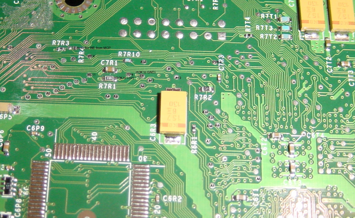
JTAG pins 'n' stuff
For the curious and the hardware-minded: the xbox motherboard is
a 4-layer board. so most signals ought to be on the outside of the board,
and you sholud be able to read it like a book. A
Mobile Celeron in BGA2 package is used, although I really
didn't find a Mobile Celeron that runs at 733/133 in a BGA2 package...
the FSB is always 100 MHz for the BGA2 packaged devices. A mystery...
the FCBGA package almost looks nicer to lay out too, it has the
same pin pitch as the BGA2 but it has a hollowed out center in which
you can stick decoupling caps. Maybe the pinout of the FCBGA
just wasn't optimal for the particular layout they were doing (with
the Nvidia northbridge on four layers) or the xbox was designed before
intel had released the FCBGA specs but microsoft really really
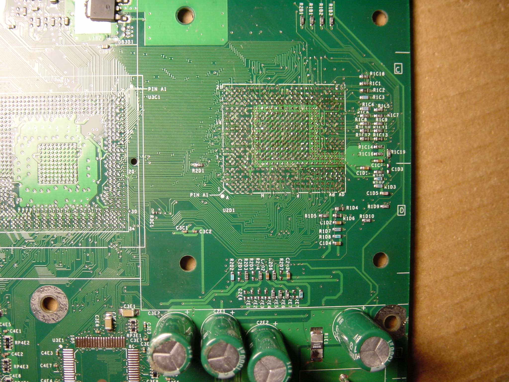
wanted a 133 MHz FSB device. Who knows...anyways, you can find a pic
of the motherboard without the Celeron on it below. Click on it
for a higher res version...the picture on the left is just the
Celeron region, the pic on the right calls out the JTAG pins in
case you have the toolz...
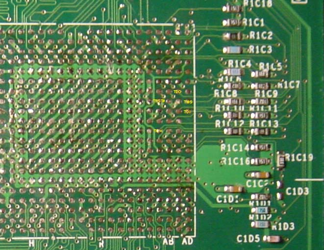
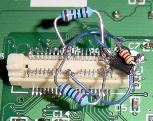
I've had a request to trace the JTAG wires out to the nearest convenient
holes or resistor pads. The image on the left shows the key JTAG pins
broken out to a set of resistors near the processor. Unfortuneately,
the TRST# signal is permanently tied to ground, at least on the
board I have. I'm not too familiar with the JTAG spec, but this
"optional" pin seems to cause the JTAG state machine to go into its
reset state. It needs to be pulsed low on power-on, but pulling it
permanently low (as it is on the Xbox) should permantently disable
the JTAG bus. Perhaps this was intentional? Who knows....but near
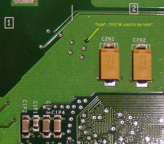
the JTAG pads I had called out in the left image, on the flip side of
the board, there is this mysterious "hole" in a poured polygon plane which
looks like someone deleted a test point or via at the last minute...perhaps
Microsoft put some thought into making the box more hack-proof than
first thought. You can see this "hole" on the right hand side image
below. If you would like to use the JTAG bus, you could just drill
out the TRST# signal (it's connected directly to an internal ground plane).
This would disconnect the TRST# signal from ground; perhaps the JTAG
state machine comes up in a recoverable manner upon power up even
if TRST# is not pulsed low. ...good luck JTAG hackers...
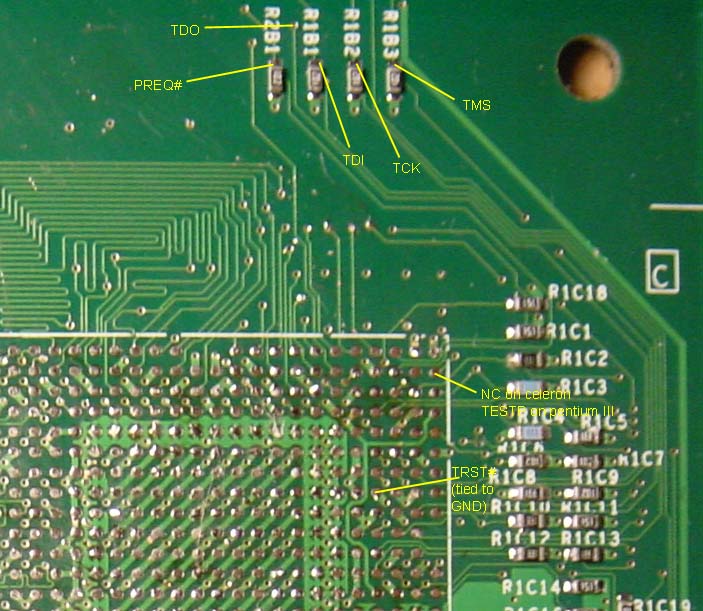
Also of note in the above picture to the left (above) is that one pin (so far as I've noticed...I haven't gone through and tracked through every pin!) nominally called out as "no connect" on the celeron pinout is actually connected to something. Note that on the Pentium III, the pin is known as "TESTP". This hints that perhaps the die used in the Xbox is a closer relative to the Pentium III perhaps???? The reason why I speculate on this is that there is no "official" Celeron with a 133 MHz FSB in a BGA2 package according to the Intel website.
For the record, I have now recovered two FLASH ROM images from two different Xboxes. They are identical. This is significant because there were some theories that each ROM image was uniquely encrypted and/or downloaded into the box by microsoft at burn-in time (some forums have noted that Xbox field service centers plug the boxes into the net and some mysterious data is sent to or from (assumedly) Microsoft). So, at least, there is *some* evidence that the ROMs may all be identical on all the xboxes...
Die Shots 'n' stuff
My girlfriend and I spent friday night in the lab together (so romantic--she's cool like that :-) and have now decapsulated three of the chips on the xbox: the southbridge (MCPX-1), the GPU (NV2A), and the Celeron. They all look like...very modern chips (unfortuneately). In other words, the high-level metal power busses criss-cross the entirety of the chip, obscuring most of the otherwise "interseting" features underneath. I don't really feel like removing the passivation and metallization, so I'll leave them as such. I haven't looked too closely yet but I don't see too many candidate regions for the high-level metal (and thus coarse pitch and easier/cheaper for mask iterations in case of code changes) ROM structure that I was hoping for. The overlay ROM that is currently foiling efforts at decrypting/modifying the BIOS ROM is probably buried in the M1 or poly layers of the chip. Ah well...it was fun taking them apart anyways. Next step: tap the LDT bus...going for the minimum path of resistance with maximum enjoyment/fun factor... although tapping the SDRAM busses might be a more direct way of getting to the decrypted code, I really don't feel like soldering hundreds of wires to the board :)
Die shots, for the curious:
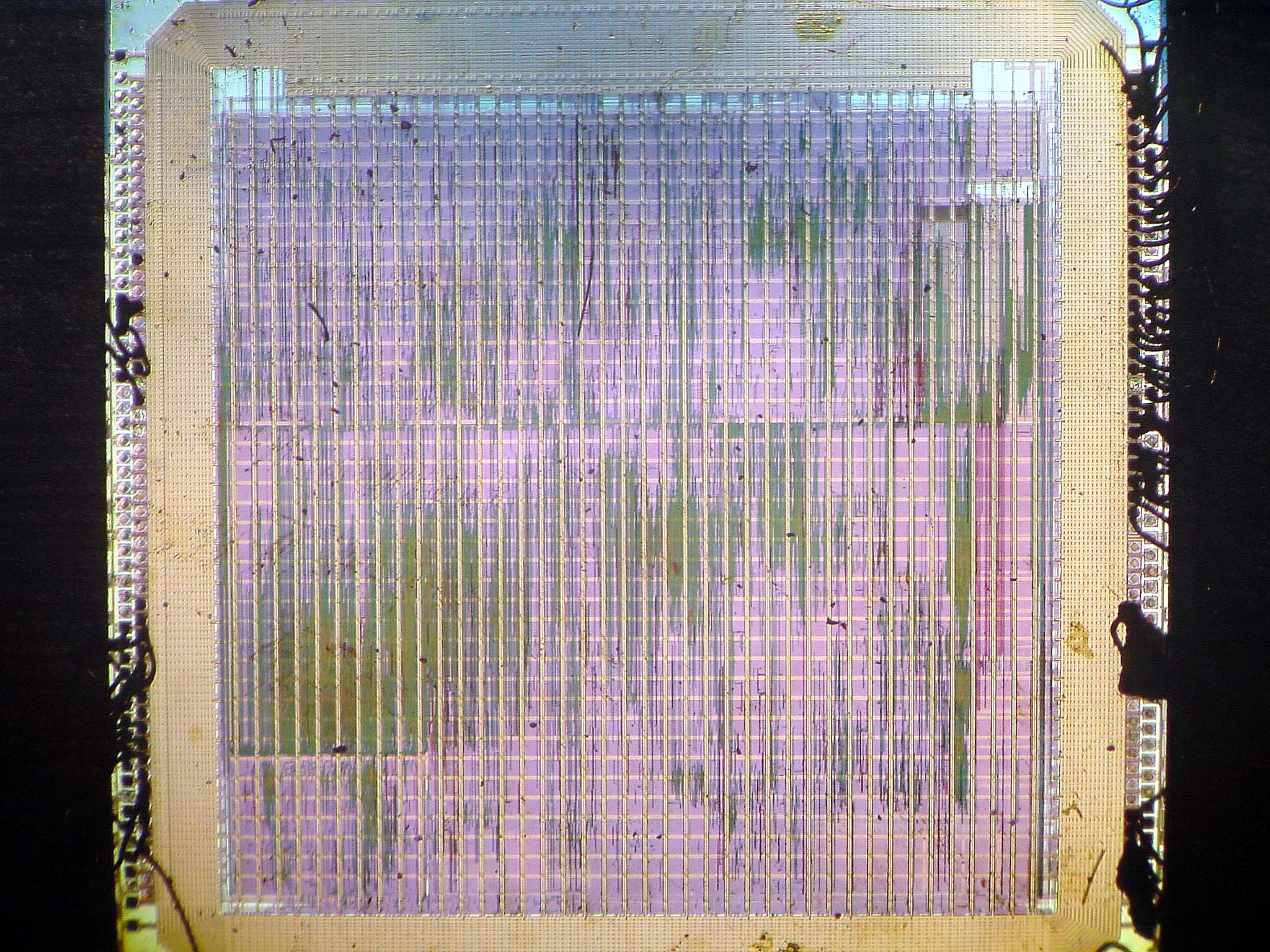
MCPX full die shot
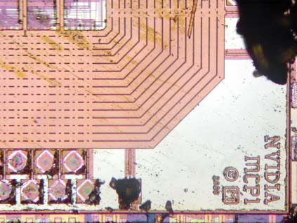
MCPX logo
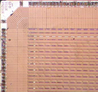
NV2A logo
Unfortuneately, I have yet to find any neat easter-eggs on the chips.
Die stats for the econmically minded: