Lecture 2:
Atomistic modeling of metals and application to the mechanics of ultra thin copper films deposited on substrates
 Copy of slides Copy of slides In this second lecture of the series entitled “From nano to macro: Introduction to atomistic modeling techniques”, we present an introduction into atomistic modeling techniques to describe plastic deformation of metals and alloys. Atomistic methods based on multi-body potentials within the EAM or MEAM framework have proven to be a quite powerful concept to understand the physical basis for deformation mechanisms of metals and similar materials. We start with a brief review of atomistic modeling techniques and numerical implementation. We continue with a historical perspective of the development of interatomic potentials for metals, starting from simple pair potentials to modern EAM or MEAM formulations. We further introduce the theoretical concepts of ductile deformation mechanisms, including a brief review of continuum theory of dislocations and experimental techniques and results. The goal is to provide a thorough review and description of the fundamentals and current state of the art of atomistic modeling techniques for metals.
In the second part, we present application of atomistic modeling techniques to describe the mechanical behavior of ultra thin copper films deposited on substrates. Through close collaboration with experimental groups, we have established a sound theoretical understanding of the deformation behavior of thin metal films at nanoscale. A key discovery is that in small-scale and nanocrystalline materials, diffusional mechanisms compete with dislocation based plasticity, and in some cases completely govern the deformation behavior. This finding is in contrast to the present belief that plasticity is mainly controlled by dislocation glide. Using joint continuum-atomistic studies, we have discovered a new class of defects called the grain boundary diffusion wedge. The diffusion wedges can be formed either by mass transport between free surfaces and grain boundaries, or by absorption of dislocations into grain boundaries as it occurs during deformation of polycrystalline metals. In thin films on substrates, the diffusion wedge induces crack-like singular stress field and as a result, dislocations moving on glide planes parallel to the substrate can be nucleated at the root of the grain boundary. This is unexpected because the biaxial stress field of a thin film does not create a resolved shear stress parallel to the substrate to cause parallel glide motion. Parallel glide dislocations have been verified by recent in-situ TEM experiments conducted at the Max Planck Institute. In nanocrystalline materials, diffusion wedges can lead to brittle crack propagation as the plastic deformation mechanisms are exhausted. In order to fully understand this phenomenon, we have developed a hierarchical modeling scheme in which semi-empirical interatomic EAM potentials derived from quantum mechanical calculations are used in large-scale classical molecular dynamics simulations. The results of molecular dynamics simulations are fed into a mesoscopic discrete dislocation model to simulate the complex interaction between dislocations and grain boundaries at larger length and time scales. The results of these studies compare favorably with relevant experimental data, which has led, for example, to a deformation mechanism map for thin film plasticity.
Literature and further reading
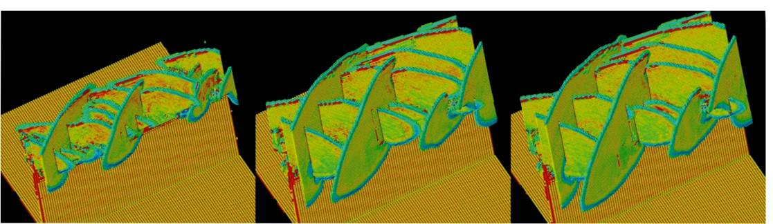
Figure: Large-scale atomistic study of nucleation of dislocations from a crack tip in copper. The dislocations shown here are nucleated from a crack with (110) surface. The visualization scheme is based on the centrosymmetry method and indicates that only partial dislocations have been nucleated (Buehlet et al., to be published). |