Solar Energy Conversion
The efficient conversion of solar radiation to electrical energy is a challenging problem with many facets and potential solutions. In the NanoEngineering group, we are approaching the problem from two angles. On one side, we are working to reduce the amount of silicon material required in crystalline silicon photovoltaics in an effort to reduce their overall cost while maintaining high efficiencies. To do this, we are developing surface structures designed to trap incident photons in thin silicon films to overcome the weak absorption of silicon that becomes problematic as the silicon thickness is reduced. In addition to photovoltaics, our group is also modeling and developing solar thermoelectric generators (STEGs), which take advantage of the entirety of the solar energy spectrum by first converting photonic energy into thermal energy and then converting thermal energy to electrical energy using a thermoelectric device.
Photovoltaics
Conventional thick-film mono- and multi-crystalline silicon solar cells are the dominant technology in the photovoltaic industry today, composing roughly 90% of all cells produced worldwide. The cost improvements associated with these technologies, however, are plateauing short of the price objectives needed to reach grid parity. One of the most persistent costs in the manufacture of wafer-based solar cells has been that of the silicon substrate, which presently accounts for 40-50% of the total module. The natural abundance of silicon suggests that the material is promising for the long-term future of photovoltaics, but it will be essential to further reduce the cost of the input materials.
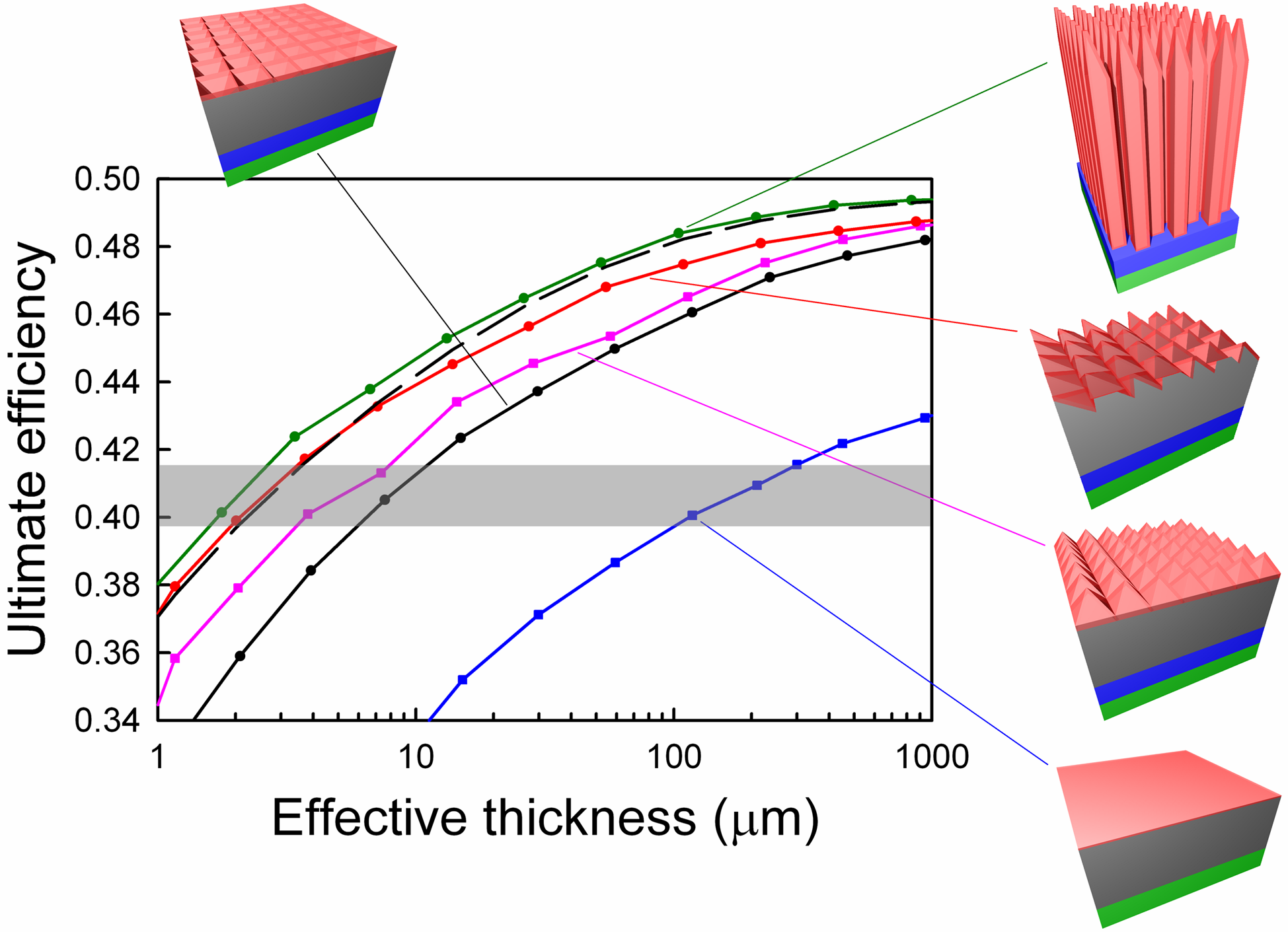
Figure 1: Click to enlarge
As an indirect bandgap material, silicon photovoltaic cells have a significant handicap in that they do not absorb light well, particularly in the red and near infrared wavelengths. Consequently, a thin silicon solar cell on a planar wafer would be quite inefficient without providing a strategy to trap photons in the material. In the NanoEngineering group, we are developing structures that overcome the low absorption coefficient of silicon by trapping light inside thin films. We are particularly interested in determining the theoretical and practical limits of photon absorption in silicon of varying thickness. Using the transfer matrix method for electromagnetic simulation, we model a variety of surface structures to identify candidates that are both manufacturable and efficient at trapping light. In Figure 1 at right, the relative absorption capability of several different structures is plotted in comparison with a planar wafer.
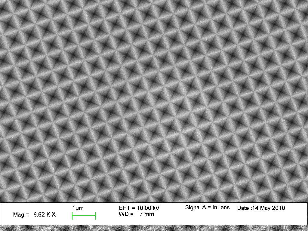
Figure 2: Click to enlarge
In addition to simulation, our group fabricates photovoltaic devices that integrate the surface structures we model with the goal of understanding how the surface structures affect overall solar cell performance. For example, Figure 2 shows a periodic, two-dimensional array of inverted pyramids on a sub-micrometer pitch fabricated using interference lithography. The bulk of the fabrication is currently done using MIT’s cleanroom facilities (MTL), but we are building our own tools to allow us to characterize the IV, quantum efficiency, and surface recombination characteristics of the solar cells we fabricate.
Solar Thermoelectrics

Figure 3: Click to enlarge
Thermoelectric generators convert heat to electricity. By coupling a thermoelectric generator to a surface that absorbs solar radiation, the sun's radiation is converted into heat and then into electricity. High-performance STEGs use wavelength-selective absorbers, a vacuum enclosure, and high-ZT thermoelectric materials to maximize efficiency. So far, STEGs have shown efficiencies as high as 5%. By improving thermoelectric materials and using optical concentration, this efficiency could be increased by a factor of 2 or more. STEGs are also excellent candidates for solar hybrid systems which produce both electricity and domestic hot water.
Selected References
- Solar PV:
- S. E. Han and G. Chen, Toward the Lambertian limit of light trapping in thin nanostructured silicon solar cells, Nano Letters, Vol. 10, 4692, 2010.
- S. E. Han, A. Mavrokefalos, M. S. Branham, and G. Chen, Efficient light-trapping nanostructures in thin silicon solar cells, Proc. SPIE Micro- and Nanotechnology Sensors, Systems, and Applications III, Vol. 8031, 80310T, 2011.
- S.E. Han and G. Chen, Optical absorption enhancement in silicon nanohole arrays for solar photovoltaics, Nano Letters, Vol. 10, pp. 1012-1015, 2010.
- L. Hu and G. Chen, Analysis of Optical Absorption in Silicon Nanowire Arrays for Photovoltaic Applications, Nano Letters, v. 7, No. 11, November, pp. 3249-3252, 2007.
- Solar Thermoelectric Generators:
- D. Kraemer, K. McEnaney, M. Chiesa, and G. Chen, Modeling and optimization of solar thermoelectric generators for terrestrial applications, Solar Energy (online), 2012. [PDF]
- K. McEnaney, D. Kraemer, Z.F. Ren, and G. Chen, Modeling of concentrating solar thermoelectric generators, Journal of Applied Physics, Vol. 110, 074502, 2011.
- G. Chen, Theoretical efficiency of solar thermoelectric energy generators, Journal of Applied Physics, Vol. 109, 104908, 2011.
- D. Kraemer, B. Poudel, H.P. Feng, J.C. Caylor, B. Yu, X. Yan, Y. Ma, X.W. Wang, D. Wang, A. Muto, K. McEnaney, M. Chiesa, Z.F. Ren, and G. Chen, High-performance flat-panel solar thermoelectric generators with high thermal concentration, Nature Materials, Vol. 10, pp. 532-538, 2011.