| the Lab |
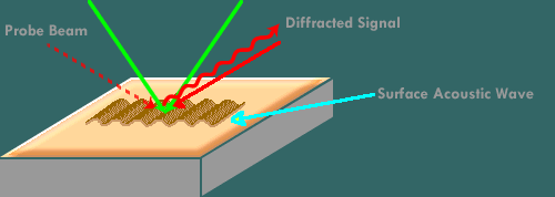
The Lambda project is currently configured to make optical measurements of thin films, especially those used in microelectronics. These films are often just a few hundred atomic layers! The experiment uses two crossed laser pulses to generate acoustic waves at the film surface. A continuous wave laser beam is then diffracted off the surface ripple resulting from the waves. The traveling wave causes the diffracted signal to oscillate in time, directly revealing the frequency and velocity of sound in the thin film. In the language of modern optical spectroscopy, this is a four-wave mixing measurement technique known as Impulsive Stimulated Thermal Scattering. A schematic view of this process is shown below.
|
 |
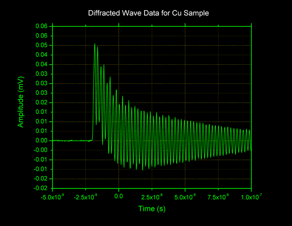
| Two sample plots, taken by Mike Maloney, are shown below.They show the frequency of surface acoustic waves in a thin film of copper [Cu] (~100 nanometers) on top of 400 nanometers of Silica, and a thin film of gold [Au] (~100 nanometers) on top of Silica. For reference, 1 nanometer is one thousandth of a millionth of a meter. |
 |
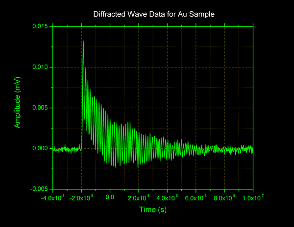 |
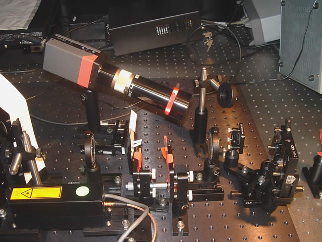
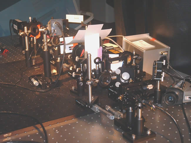
| Information about the thin film structure can be gained by measuring the frequency of the diffracted signal oscillations, which corresponds to the frequency of sound in the thin metal film. For example, the film thickness, a crucially important property for metal layers in computer chips, can be determined with angstrom precision! For more information about how the frequency of sound is sensitive to the properties of the thin metal film, and scientific papers discussing this technique in more detail, see the Resources section of this website. The experimental set-up used in the Lambda project is shown below from three different angles. If you participate in the project and carry out the experiments, you'll know what all the components do! |
| Side View |
 |
| Front View |
 |
| Back View |
 |
| |