![]()
by Andrew S. Huang, 6/28/96
Introduction
FPM DRAM, EDO DRAM, CDRAM, EDRAM, RDRAM, SDRAM, SGRAM, VRAM, WRAM, SRAM, SSRAM, SIMM, DIMM, DIP...
Do you know what all of these acronyms mean? Better yet, do you know the features of all these architectures? Well, before writing this FAQ, I was not familiar with most of these acronyms. In today's fast-paced industry with marketeers trying to gain product distinction and price premiums, the proliferation of acronyms is sometimes intimidating. I hope you find this FAQ as edifying and fun as I found it to write.
Acknowledgements, up front: most of the information presented in this
FAQ is lifted directly from databooks and magazine articles. I will cite
sources as I use them. Most pictures are scans from magazines, or lifted
from on-line databooks (thank you Micron!)--no, I didn't draw 'em myself.
If anyone finds material in this FAQ objectionable because of copyright,
send bunnie@mit.edu email, and
I'll find a suitable replacement.
![]()
DRAM
Overview
So, just what is DRAM? DRAM stands for:
The breakdown of this acronym hints at the workings underneath--some form of decaying storage, some form of addressable array. The fundamental element of a DRAM is a single capacitor-transistor element which stores 1 bit of information:
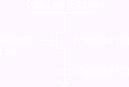
C is on the order of 1 fF (10e-15 F); at 1.6e19 electrons / coulomb, that is only about 40,000 electrons! Thus, even though the transistor has a fairly high off resistance of a few teraohms (10e12 ohms), the time constant for this circuit is on the order of milliseconds (typically tens to hundreds of milliseconds for modern designs). Also, when dealing with such tiny numbers, correctly sensing the presence or absence of charge is quite a challenge. DRAM arrays use special amplifiers, called sense amps, to detect the state of the capacitor. Once a bit has been read, it must be refreshed since reading pulls a lot of charge out of the capacitor. DRAM cells are so sensitive that stray alpha particles can induce errors (called soft errors by DRAM mfgs). I once heard that some nuclear scientists were using a massive array of DRAM chips as particle detectors! When designing with DRAM, keep in mind that it is primarily an analog part, and is quite sensitive to noise and power supply fluctuations.
Well, with a few million of these sensitive devices on a single die, one can imagine that support circuitry is required. Here is a block diagram of a typical, bare-bones DRAM array (1Megx4 FPM):
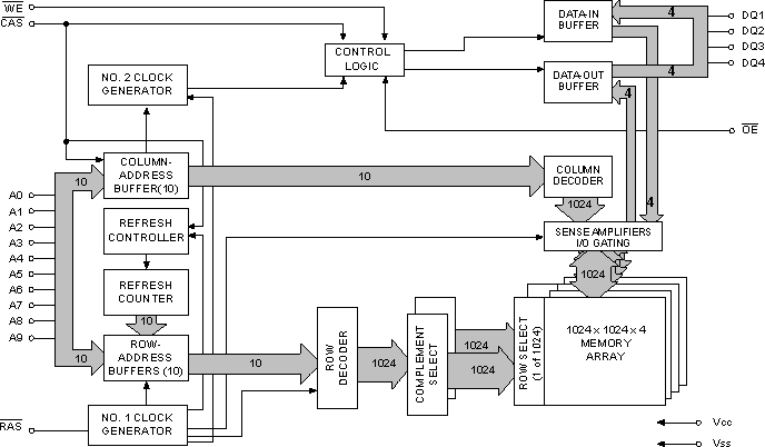
Picture from Micron on-line datasheet
The important features to glean from this diagram are:
Now that the basic DRAM structure has been introduced, I will discuss what makes the different flavors of DRAM significant. I will approach this from two directions: that of architecture, and that of timing.
Fast Page Mode DRAM is the vanilla DRAM as of June 1996, and is rapidly being replaced by other faster technologies. By the time you read this, FPM DRAM will probably be obsolete. Still, it enjoyed a huge popularity for a few years, so it is the standard against which all other DRAM architectures are compared.
Each normal DRAM access requires two address cycles, one for row address, and one for column address. A fast page mode DRAM access consists of a sequence of accesses where only the first access specifies both row and column addresses; the remainder specifies just a column address (the row address is implicity the same). This asymptotically reduces access time by 50%. If one thinks of each row of a DRAM as a page of data, one can see the etymology of the fast page nomenclature.
FPM works in a real system because there is some spatial locality of data access patterns--in general, if you grabbed data from one area, you are likely to grab more data from that area. If data access patterns were completely random, FPM would only perform marginally better than normal DRAM. This situation is analogous to someone looking for words in a dictionary; looking for words that happen to be on the same page is faster than looking for words on different pages.
Of course, in order to take advantage of FPM, the system must be designed to utilized FPM...replacing normal DRAM with FPM DRAM offers no speed improvement without system reconfiguration.
The following timing diagram illustrates an FPM access:
If you have comments, corrections, or suggestions, email me at bunnie@mit.edu
![]()
This page created with Netscape Navigator Gold (thanks, Netscape!)